Conductive layer, manufacturing method of the same, and signal transmission substrate

a technology of conductive layer and manufacturing method, which is applied in the direction of fixed connection, semiconductor/solid-state device details, coupling device connection, etc., can solve the problems of reducing the yield of diagnostic vests, requiring the manufacture of diagnostic vests, and difficulty in precisely aligning the low electrical resistance layer. achieve the effect of improving the accuracy of alignmen

Inactive Publication Date: 2010-03-02
HOYA CORP
View PDF12 Cites 62 Cited by
  • Summary
  • Abstract
  • Description
  • Claims
  • Application Information

AI Technical Summary

Benefits of technology

[0006]The present invention is advantageous in that a method of manufacturing a conductive layer used in a signal transmission substrate configured to enhance the accuracy of alignment between high and low electrical resistance portions is provided, and / or a conductive layer formed in accordance with the manufacturing method is provided, and and / or a signal transmission substrate having the conductive layer is provided.
[0008]By manufacturing the conductive layer in accordance with the above mentioned method, it is possible to easily align the plurality of low resistance regions with the high resistance region. Therefore, easiness of manufacturing of the conductive layer and positioning accuracy of the low resistance regions can be enhanced. By employing conductive thread as material of the low resistance region, it is possible to form a conducive layer without laminating a low resistance layer and a high resistance layer together. Therefore, a layer structure of the signal transmission structure can be simplified.
[0013]Such a configuration makes it possible to simplify a layer structure of the signal transmission structure.
[0026]Such a configuration makes it possible to simplify a layer structure of the signal transmission structure.

Problems solved by technology

However, if a member having extensibility (e.g., fabric) is used for each layer of the diagnostic vest, a yield of diagnostic vests may decrease because of a trouble which may be caused in a manufacturing process of diagnostic vests.
For example, if a low electrical resistance layer is formed of fabric having conductivity and extensibility and a high electrical resistance layer is formed of fabric having an insulating property and extensibility, it is difficult to exactly align the low electrical resistance layer with the high electrical resistance layer to laminate these layers together because these layers do not have rigidity.
Therefore, a manufacturer of diagnostic vests is required to reduce the accuracy of alignment between the low and high electric resistance layers, or to conduct a screening test for screening out defectives.

Method used


Image

  • Conductive layer, manufacturing method of the same, and signal transmission substrate
  • Conductive layer, manufacturing method of the same, and signal transmission substrate
  • Conductive layer, manufacturing method of the same, and signal transmission substrate

Examples


first embodiment

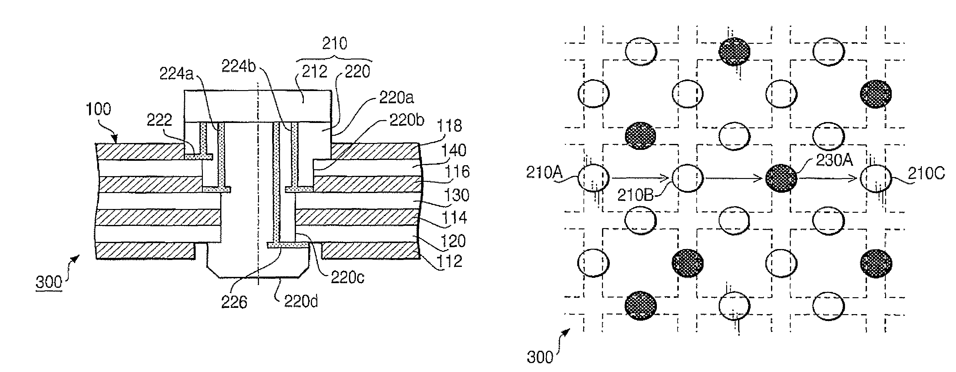
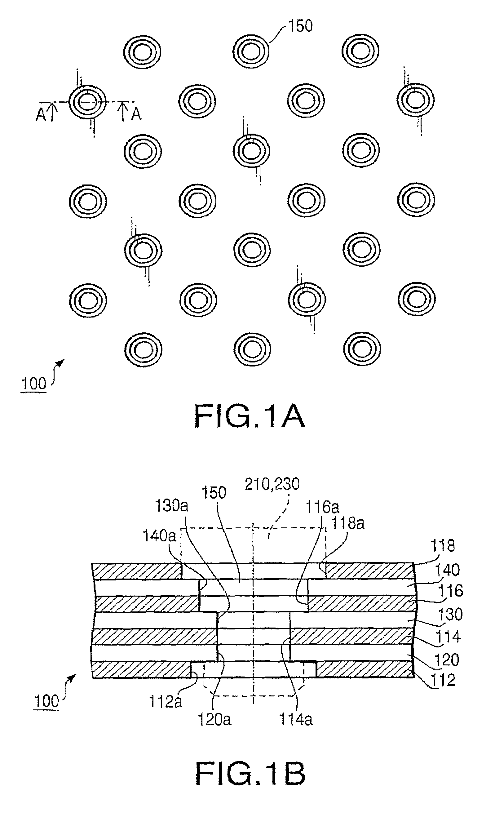
[0048]FIG. 1A is a plan view of a signal transmission substrate 100 according to a first embodiment. FIG. 1B is a cross-sectional view of the signal transmission substrate 100 along a line A-A in FIG. 1A. The signal transmission substrate 100 is employed in a communication device 300 (see FIGS. 4 and 5). The signal transmission substrate 100 has a laminated structure of seven layers including an insulating layer 112, a ground layer 120, an insulating layer 114, a signal layer 130, an insulating layer 116, a power layer 140, and an insulating layer 118 from the bottom.

[0049]Each of the insulating layers 112, 114, 116 and 118 is formed of, for example, fabric having flexibility, extensibility and an insulating property. The insulating layer 112 insulates the ground layer 120 from the outside, the insulating layer 114 insulates the signal layer 130 from the ground layer 120, the insulating layer 116 insulates the signal layer 130 from the power layer 140, and the insulating layer 118 i...

second embodiment

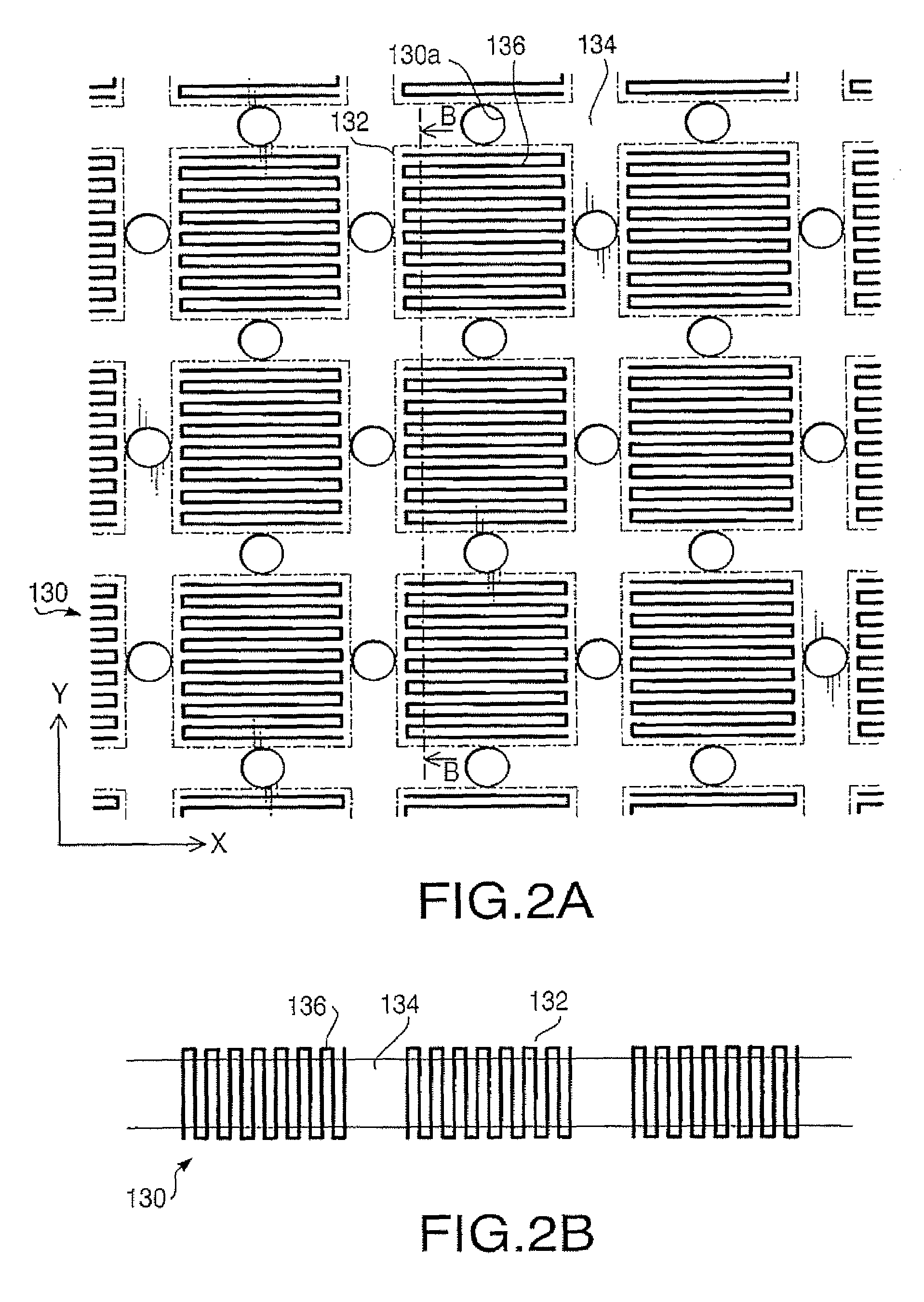
[0085]FIG. 7 is a partial top view of the signal layer 130B of a signal transmission substrate according to a second embodiment. In the second embodiment, the conductive thread 136 is sewed in the fabric forming the high resistance region 134 so that lines of the conductive thread 136 are elongated both in the X and Y directions in a low resistance region 132z. In this embodiment, each low resistance region 132z is formed in two sewing processes. The two sewing processes include a first process of sewing the conductive thread 136 in the fabric to form lines of the conductive thread 136 extending in the X direction, and a second process of sewing the conductive thread 136 in the fabric to form lines of the conductive thread 136 extending in the Y direction perpendicularly intersecting with the X direction. The first process may be performed ahead of the second process, or the second process may be performed ahead of the first process.

[0086]In this embodiment, the lines of the conduct...

third embodiment

[0088]FIG. 8 is a partial top view of a signal layer 130C of a signal transmission substrate according to a third embodiment. In the third embodiment, the conductive thread 136 is sewed in the fabric forming the high resistance region 134 so that a spiral pattern of the conductive thread 136 is formed in each low resistance region 132y. The low resistance region 132y may be formed by a single sewing process of sewing the conductive thread 136 in the low resistance region 132y to form a spiral pattern. Since lines of the conductive thread 136 extending both in the X and Y directions can be formed in a single sewing process, the manufacturing process can be reduced in comparison with the case of the sewing process of the second embodiment.


PUM


Abstract

There is provided a method of manufacturing a conductive layer of in a signal transmission substrate. The method includes sewing conductive thread in sheet-like material having an insulating property so as to form one of a plurality of low resistance regions using the conductive thread in a high resistance region formed by the sheet-like material, moving the conductive thread from an end point of a previously sewed low resistance region to a start point of a low resistance region to be sewed subsequently, repeating the sewing and moving steps to form the plurality of low resistance regions in the high resistance region, and forming a plurality of holes in the conductive layer by press working so that an electrical component attached to at least one of the plurality of holes is able to transmit a signal between neighboring ones of the plurality of low resistance regions.

Description

BACKGROUND OF THE INVENTION[0001]The present invention relates to a configuration of a conductive layer to be employed in a signal transmission substrate for transmitting a signal in accordance with a two dimensional Diffusive Signal-Transmission technology.[0002]Recently, a technology for transmitting a signal (a packet) to a destination via a plurality of DST (Diffusive Signal-Transmission) chips has been proposed as described in Japanese Patent Provisional Publication No. 2004-328409 (hereafter, referred to as JP 2004-328409A) and on a web site “http: / / www.utri.co.jp / venture / venture2.html” (retrieved in November, 2005) by CELLCROSS Co., Ltd (the same contents are also available on the website http: / / www.cellcross.co.jp / technology.html). Hereafter, such a technology is referred to as a 2D-DST (two-dimensional DST) technology.[0003]In JP 2004-328409A, a communication device having a conductive layer configured to include a plurality of low electrical resistance layers and high elec...

Claims


Application Information

Patent Timeline
Patent Type & Authority Patents(United States)
IPC IPC(8): H01R33/00H01R12/50
CPCH05K1/0287H05K3/103H05K2201/0715H05K2201/09263H05K2201/09609H05K2201/10287H05K2201/10598
Inventor ITO, EIICHITSUDA, KOJIMINAKUCHI, TADASHIMATSUMOTO, MITSUHIRO
Owner HOYA CORP
Why Eureka
Try Eureka