Multi-domain vertical alignment liquid crystal display panel

a vertical alignment and liquid crystal display technology, applied in non-linear optics, instruments, optics, etc., can solve the problems of insufficient wideness of conventional liquid crystal displays, improve the problem of poor liquid crystal arrangement or low aperture ratio, and reduce the quantity of protruding protruding

Active Publication Date: 2010-03-02
AU OPTRONICS CORP
View PDF14 Cites 8 Cited by
  • Summary
  • Abstract
  • Description
  • Claims
  • Application Information

AI Technical Summary

Benefits of technology

[0008]It is an objective of the present invention to provide a multi-domain vertical alignment liquid crystal display panel for improving the problem of poor liquid crystal arrangement or low aperture ratio caused by the increased number of protrusions.
[0009]Specifically, the protrusions of the present invention are disposed on the top substrate where correspond to the scan lines or the data lines, such that the quantity of protrusions can be reduced significantly while fabricating high resolution liquid crystal displays. Additionally, a plurality of main slits is formed in the pixel electrode and the quantity of protrusions is reduced to increase the aperture ratio of the display panel, increase the stability of the liquid crystal arrangement, reduce the opportunity of light leakage during dark state and increase the overall contrast.

Problems solved by technology

However, the viewing angle of a conventional liquid crystal display is not wide enough to ensure a high display quality, therefore, multi-domain vertical alignment (MVA) liquid crystal displays capable of orientating liquid crystals in various directions are proposed to improve the above problem.

Method used


Image

  • Multi-domain vertical alignment liquid crystal display panel
  • Multi-domain vertical alignment liquid crystal display panel
  • Multi-domain vertical alignment liquid crystal display panel

Examples


first embodiment

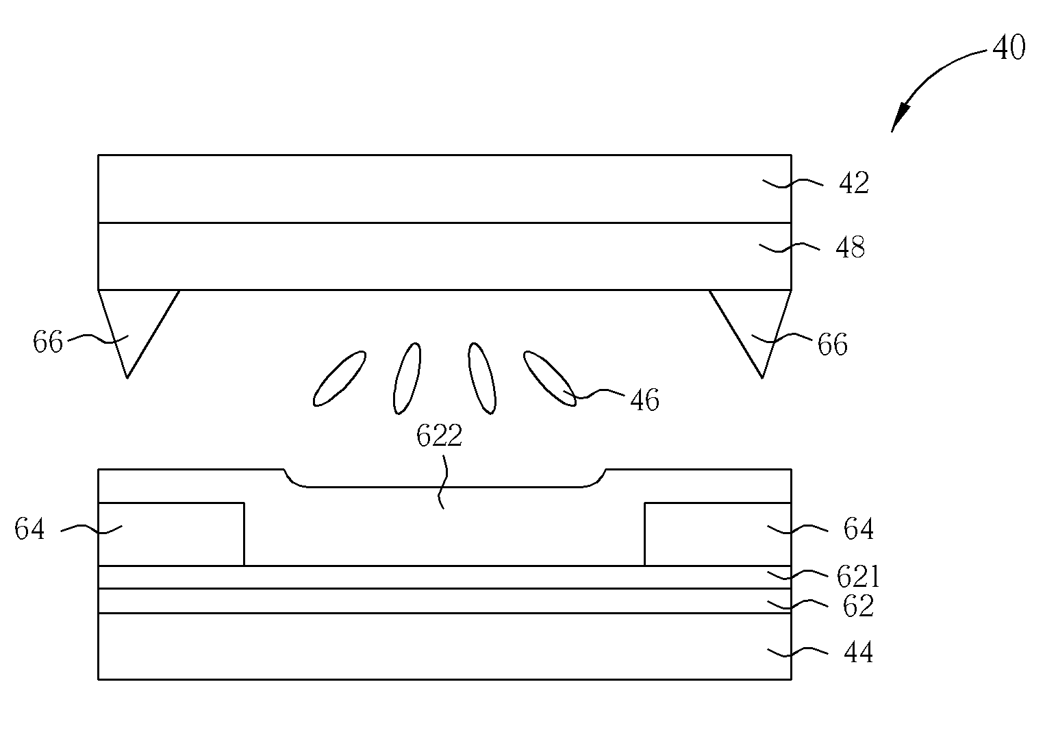
[0030]Please refer to FIG. 3. FIG. 3 illustrates a cross-sectional view of an MVA LCD panel 40 according to the first embodiment of the present invention. As shown in FIG. 3, the MVA LCD panel 40 includes a top substrate 42, a bottom substrate 44, a liquid crystal layer 46 disposed between the top substrate 42 and the bottom substrate 44, a common electrode 48 disposed on the top substrate 42, a color filter 45 disposed between the top substrate 42 and the common electrode 48, a plurality of protrusions 52 disposed on the common electrode 48, and a plurality of thin film transistors (not shown) and pixel electrodes 58 disposed on the bottom substrate 44. The liquid crystal layer 46 can be composed of negative or positive liquid crystals. Alternatively, the color filter 45 can be formed on the bottom substrate 44 to form a color filter on array substrate, which are all within the scope of the present invention.

[0031]Please refer to FIGS. 4-6. FIG. 4 illustrates a plan view of a pixel...

second embodiment

[0033]Please refer to FIG. 7. FIG. 7 illustrates a plan view of a pixel unit 80 of the MVA LCD panel according to the second embodiment of the present invention. As shown in FIG. 7, the MVA LCD panel includes a pixel unit 80, a plurality of scan lines 82 and data lines 84 disposed around the pixel unit 80, and a plurality of protrusions 86 disposed on the top substrate where correspond to the scan lines 82 and data lines 84. The pixel unit 80 is driven by a switch element 83 electrically connected to the scan lines 82, the data lines 84, and the pixel electrode 88, in which the switch element 83 is preferably a thin film transistor.

[0034]The pixel unit 80 includes a pixel electrode 88 having a plurality of main slits 89. Depending on the design of the product, the main slits 89 can be formed in the pixel electrode 88 or extended to the edge of the pixel electrode 88. In contrast to the first embodiment, the left protrusions 86 of the second embodiment are positioned corresponding to...

third embodiment

[0035]Please refer to FIG. 8. FIG. 8 illustrates a plan view of a pixel unit 90 of the MVA LCD panel according to the third embodiment of the present invention. As shown in FIG. 8, the MVA LCD panel includes a pixel unit 90, a plurality of scan lines 92 and data lines 94 disposed around the pixel unit 90, and a plurality of protrusions 96 disposed on the top substrate where correspond to the scan lines 92 and data lines 94. The pixel unit 90 is driven by a switch element 93 electrically connected to the scan lines 92, the data lines 94, and the pixel electrode 98, in which the switch element 93 is preferably a thin film transistor.

[0036]The pixel unit 90 includes a pixel electrode 98 having a plurality of main slits 97 and fine slits 99. Depending on the design of the product, the main slits 97 and the fine slits 99 can be formed in the pixel electrode 98 or extended to the edge of the pixel electrode 98. Similar to the second embodiment of the present invention, the left protrusion...


PUM

PropertyMeasurementUnit
circular shapeaaaaaaaaaa
stabilityaaaaaaaaaa
sizeaaaaaaaaaa

Abstract

A liquid crystal display panel is disclosed. The liquid crystal display panel includes a bottom substrate, a plurality of wires disposed on the bottom substrate, a plurality of pixel units electrically connected to the wires, a top substrate disposed opposite to the bottom substrate, a liquid crystal layer disposed between the top and bottom substrates, and at least one protrusion disposed on the top substrate corresponding to the wires formed between two adjacent pixel units. Each pixel unit includes a thin film transistor and a pixel electrode disposed on the bottom substrate. The pixel electrode is electrically connected to the thin film transistor, in which the pixel electrode has a plurality of main slits.

Description

BACKGROUND OF THE INVENTION[0001]1. Field of the Invention[0002]The invention relates to a liquid crystal display panel, and more particularly, to a multi-domain vertical alignment liquid crystal display panel.[0003]2. Description of the Prior Art[0004]Liquid crystal displays (LCDs) are commonly utilized in various electronic products including cell phones, PDAs, and notebook computers. As the market demand for flat display panels continues to increase, liquid crystal displays become popular due to the advantages such as thin and lightweight. In fact, liquid crystal displays are gradually replacing cathode ray tube (CRT) displays that had dominated the market for so many years. However, the viewing angle of a conventional liquid crystal display is not wide enough to ensure a high display quality, therefore, multi-domain vertical alignment (MVA) liquid crystal displays capable of orientating liquid crystals in various directions are proposed to improve the above problem.[0005]Please ...

Claims


Application Information

Patent Timeline
Patent Type & Authority Patents(United States)
IPC IPC(8): G02F1/1337G02F1/1335G02F1/1343
CPCG02F1/133707G02F1/1393G02F2001/134345G02F1/134345
Inventor SU, MU-JENCHANG, CHIH-MING
Owner AU OPTRONICS CORP
Why Eureka
Try Eureka