
Eureka
For R&D, Eureka makes reading and utilizing patents & technical documents easy.
Eureka AIR
Designed for self-driven R&D workflows. Generate viable solutions, solve complex R&D challenges, empower your innovation with AI.

Eureka Materials
Designed for material experts only. Revolutionize your material R&D, from search, analyze, to developing new materials.

TechResearch
Generate reliable direction feasibility study reports for your R&D in just a few steps.

TechSeek
Discover and master advanced knowledge NOW. Basics, ideas, possibilities, all at once.

TechMind
As an expert in R&D Theories, TechMind can generates customized viable solutions instantly.

TechRisk
Analyze your overall solution with one click, know your potential R&D risks in advance.

TechMonitor
Get weekly tech updates, stay abreast of the latest tech innovations and key insights.
Semiconductor integrated device, method of designing semiconductor integrated device, device for designing the same, and program
a technology of integrated devices and semiconductors, applied in the field of semiconductor integrated devices, can solve the problems of inability to increase inability to completely short circuit wires or vias, and inability to integrate into a large pattern, etc., to achieve the effect of increasing the integration level of a pattern in a semiconductor integrated devi
- Summary
- Abstract
- Description
- Claims
- Application Information
AI Technical Summary
Benefits of technology
Problems solved by technology
Method used
Image

Examples
first embodiment
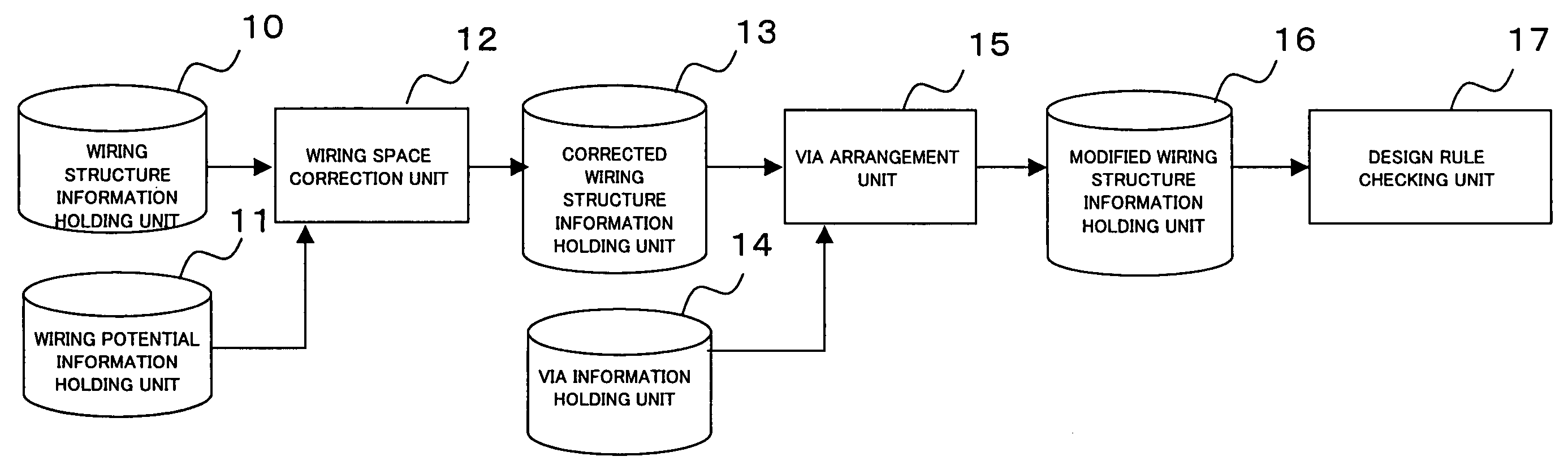
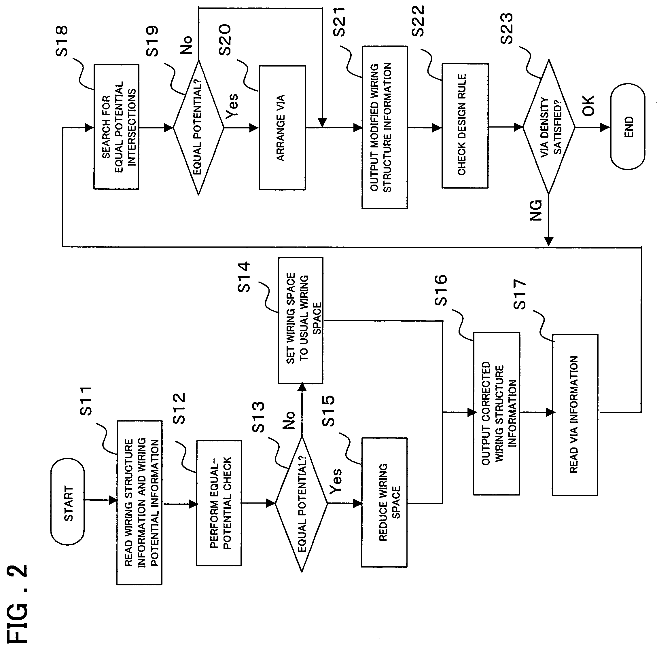
[0040]FIG. 2 is a flowchart showing the design method of a semiconductor integrated device in a first embodiment of the present invention. The following primarily describes how an automatic wiring program wires a wide wire such as a power wire. A fine signal wire is wired after the processing in FIG. 2 is terminated.
[0041]In step S11 in FIG. 2, the program reads a file, which pre-stores therein the wiring structure information on a semiconductor integrated device for which wiring is to be laid out, from the wiring structure information holding unit 10. The wiring structure information file stores information on the wiring structure wired by a conventional automatic wiring program that does not consider whether the potential is equal between wires. Note that the wiring structure information file includes information on the structure where vias are not yet arranged. The program also reads potential information on the wires of the semiconductor integrated device from the wiring potenti...
second embodiment
[0063]FIG. 4 is a flowchart showing the design method for a semiconductor integrated device in a second embodiment of the present invention. In FIG. 4, the same processing is performed for the same reference numeral in FIG. 2 and repetitive description will not be given.
[0064]In step S17a in FIG. 4, the program reads information from the two files: one is the via information file that stores the number of vias, which connect the equal-potential intersections between power layers, and arrays, and the other is the via density information file that defines the via-dense areas.
[0065]In step S25, a determination is made as to whether the arranged via satisfies the via density criterion. If the via density criterion is satisfied (OK), control is passed to step S21; if the via density criterion is not satisfied (NG), control is passed to step S26.
[0066]In step S26, the wiring space is expanded to satisfy the via density criterion and control is passed to step S20 to confirm that the via de...
PUM
 Abstract
Description
Claims
Application Information
 - R&D Engineer
- R&D Manager
- IP Professional
- Industry Leading Data Capabilities
- Powerful AI technology
- Patent DNA Extraction
Browse by: Latest US Patents, China's latest patents, Technical Efficacy Thesaurus, Application Domain, Technology Topic, Popular Technical Reports.
© 2024 PatSnap. All rights reserved.Legal|Privacy policy|Modern Slavery Act Transparency Statement|Sitemap|About US| Contact US: help@patsnap.com