
High integrated open bit line structure semiconductor memory device with precharge units to reduce interference or noise

a semiconductor memory device and pre-charge unit technology, applied in the field of semiconductor memory devices with high integrated open-bit line structure semiconductor memory devices to reduce interference or noise, to achieve the effect of reducing the layout size of the semiconductor memory devices

Active Publication Date: 2010-03-23
SK HYNIX INC
View PDF7 Cites 3 Cited by
  • Summary
  • Abstract
  • Description
  • Claims
  • Application Information

AI Technical Summary

Benefits of technology

[0014]It is an object of the present invention to provide a semiconductor memory device having a 6F2 open bit line structure which connects each of a bit line pair to each of a neighboring bit line pair for a precharge operation so that a layout size of the semiconductor memory device decreases.

Problems solved by technology

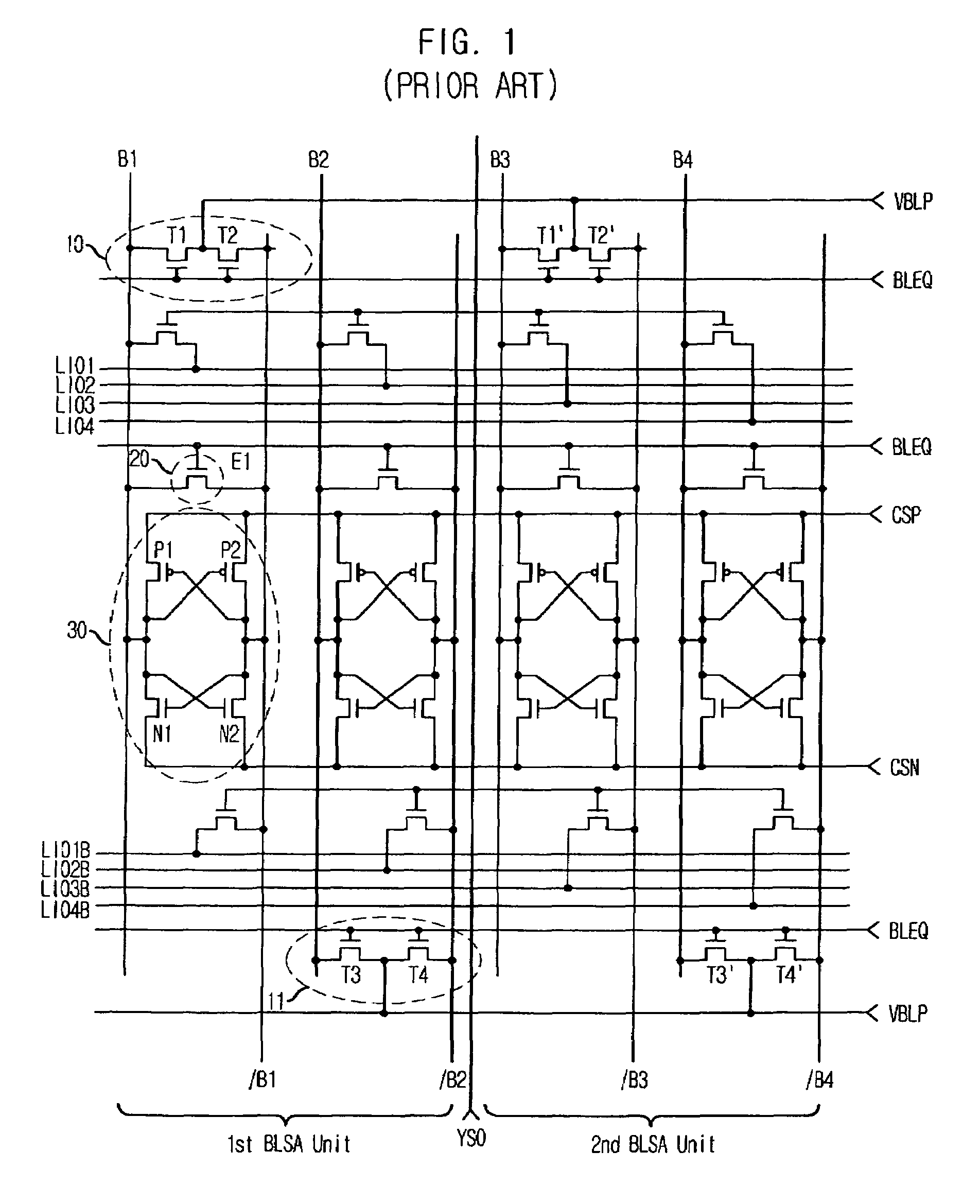
At issue for higher integration is how to make a minuter pattern in the semiconductor memory device.

Method used


Image

  • High integrated open bit line structure semiconductor memory device with precharge units to reduce interference or noise
  • High integrated open bit line structure semiconductor memory device with precharge units to reduce interference or noise
  • High integrated open bit line structure semiconductor memory device with precharge units to reduce interference or noise

Examples


Embodiment Construction

[0021]Hereinafter, a semiconductor memory device in accordance with specific embodiments of the present invention will be described in detail with reference to the accompanying drawings.

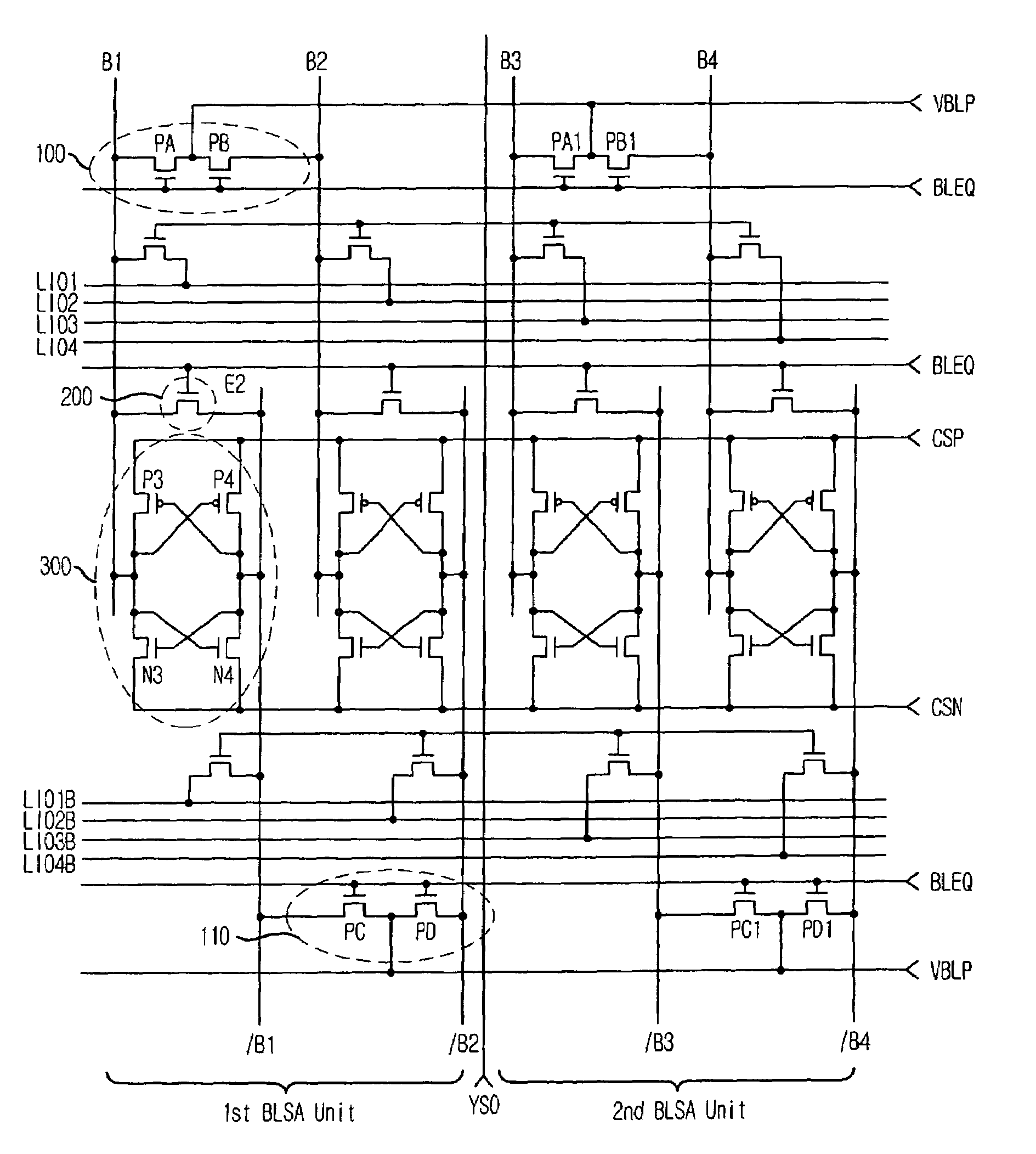
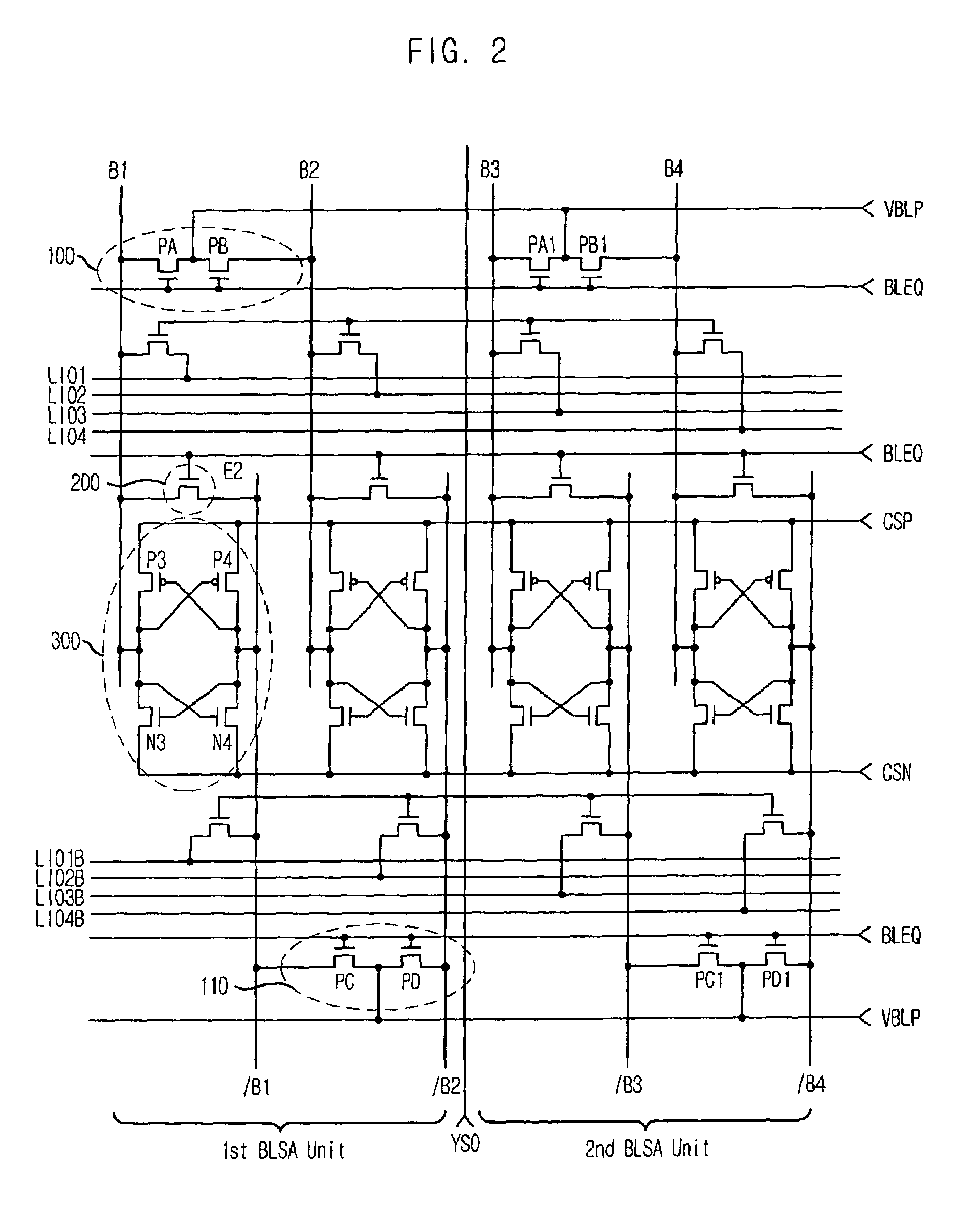
[0022]FIG. 2 is a schematic circuit diagram of a sense amplifying block included in a semiconductor memory device in accordance with the present invention.

[0023]The sense amplifying block includes first and second precharge units 100 and 110, an equalizing unit 200, and a sense amplifier 300.

[0024]The first precharge unit 100 precharges one of a first bit line pair B1 and / B1 and one of a second bit line pair B2 and / B2 in response to a bit line equalizing signal VBLP. The second precharge unit 110 precharges the other of the first bit line pair B1 and / B1 and the other of the second bit line pair B2 and / B2 in response to the bit line equalizing signal VBLP. Particularly, in FIG. 2, the first precharge unit 100 precharges a first bit line B1 and a second bit line B2 and the second precharge unit 110...


PUM


Abstract

A semiconductor memory device, having a 6F2 open bit line structure, connects each bit line of a bit line pair to a respective bit line of a neighboring bit line pair for a precharge operation so that a layout size of the semiconductor memory device decreases. Plural first precharge units each precharge one bit line of a first bit line pair and one bit line of a second bit line pair in response to a bit line equalizing signal. Plural sense amplifiers each sense a data bit supplied to a respective one of the first and second bit line pairs and amplify sensed data.

Description

FIELD OF INVENTION[0001]The present invention relates to a semiconductor memory device; and, more particularly, to a high integrated sense amplifier of which layout size can be reduced in a semiconductor memory device having an open bit line structure.DESCRIPTION OF RELATED ARTS[0002]Integration and capability of a semiconductor memory device is continuously being enhanced. There are two issues that are primarily addressed: increasing the speed at which the semiconductor memory device can operate, and increasing data storage capability of the semiconductor memory device in a restricted area.[0003]As storage capacity of the semiconductor memory device increases, a larger area is required and / or higher integration. At issue for higher integration is how to make a minuter pattern in the semiconductor memory device. A fold bit line structure (generally, referred as to an 8F2 cell structure) and an open bit line structure (generally, referred as to a 6F2 cell structure) have been suggest...

Claims


Application Information

Patent Timeline
Patent Type & Authority Patents(United States)
IPC IPC(8): G11C7/00
CPCG11C7/12G11C7/18G11C11/419G11C7/06
Inventor WON, HYUNG-SIK
Owner SK HYNIX INC
Learn More