Auto-gain correction and common mode voltage cancellation in a precision amplifier

a technology of precision amplifier and gain correction, which is applied in the direction of amplifiers, amplifiers with semiconductor devices/discharge tubes, amplifiers, etc., can solve the problems of input offset, method of obtaining gain accuracy, and physical imperfections in the accuracy of linear amplifier dc outpu

Active Publication Date: 2010-04-13
MAXIM INTEGRATED PROD INC
View PDF6 Cites 34 Cited by
  • Summary
  • Abstract
  • Description
  • Claims
  • Application Information

AI Technical Summary

Problems solved by technology

The accuracy of the DC output of a linear amplifier is subject to the physical imperfections of the individual devices comprising the amplifier.
In an integrated circuit, input offsets are a result of minor defects and minor device mismatches in amplifier gain stages.
Conversely, methods to obtain gain accuracy have usually required the need for trimming, and usually do not obtain gain accuracy over a wide temperature range or a wide input common mode voltage range, where the input common mode voltage is the average of the two differential inputs relative to a common ground.
One source of Gain Error involves the accuracy of the feedback.
The ...

Method used


Image

  • Auto-gain correction and common mode voltage cancellation in a precision amplifier
  • Auto-gain correction and common mode voltage cancellation in a precision amplifier
  • Auto-gain correction and common mode voltage cancellation in a precision amplifier

Examples


Embodiment Construction

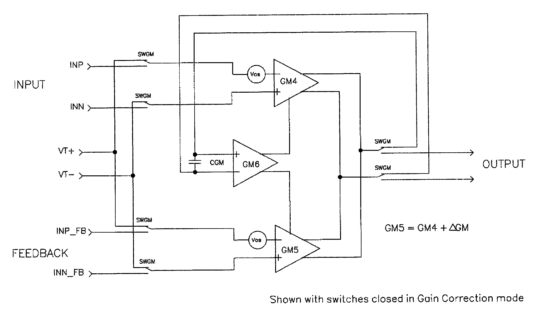
[0026]The present invention provides a means for continually calibrating the gain of the two differential input stages relative to each other and thus significantly minimizes the effects of semiconductor device mismatch, temperature and common mode input voltage. Embodiments of this invention also make use of auto-zero techniques in conjunction with chopper-stabilized techniques to eliminate trim and effectively reduce gain error associated with the matching of the two differential input stages.

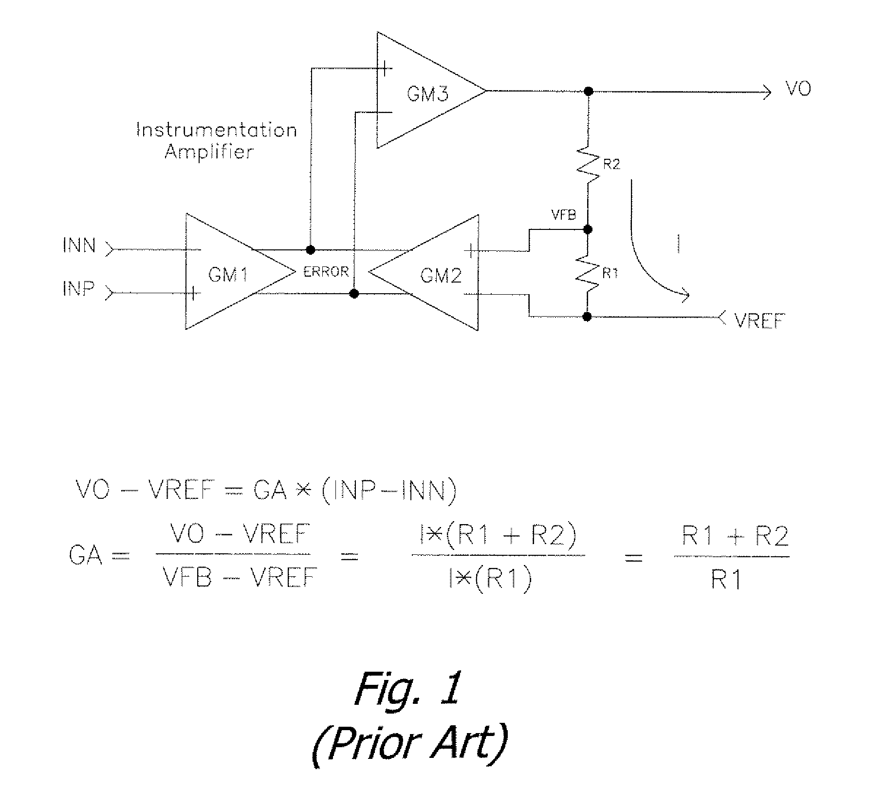
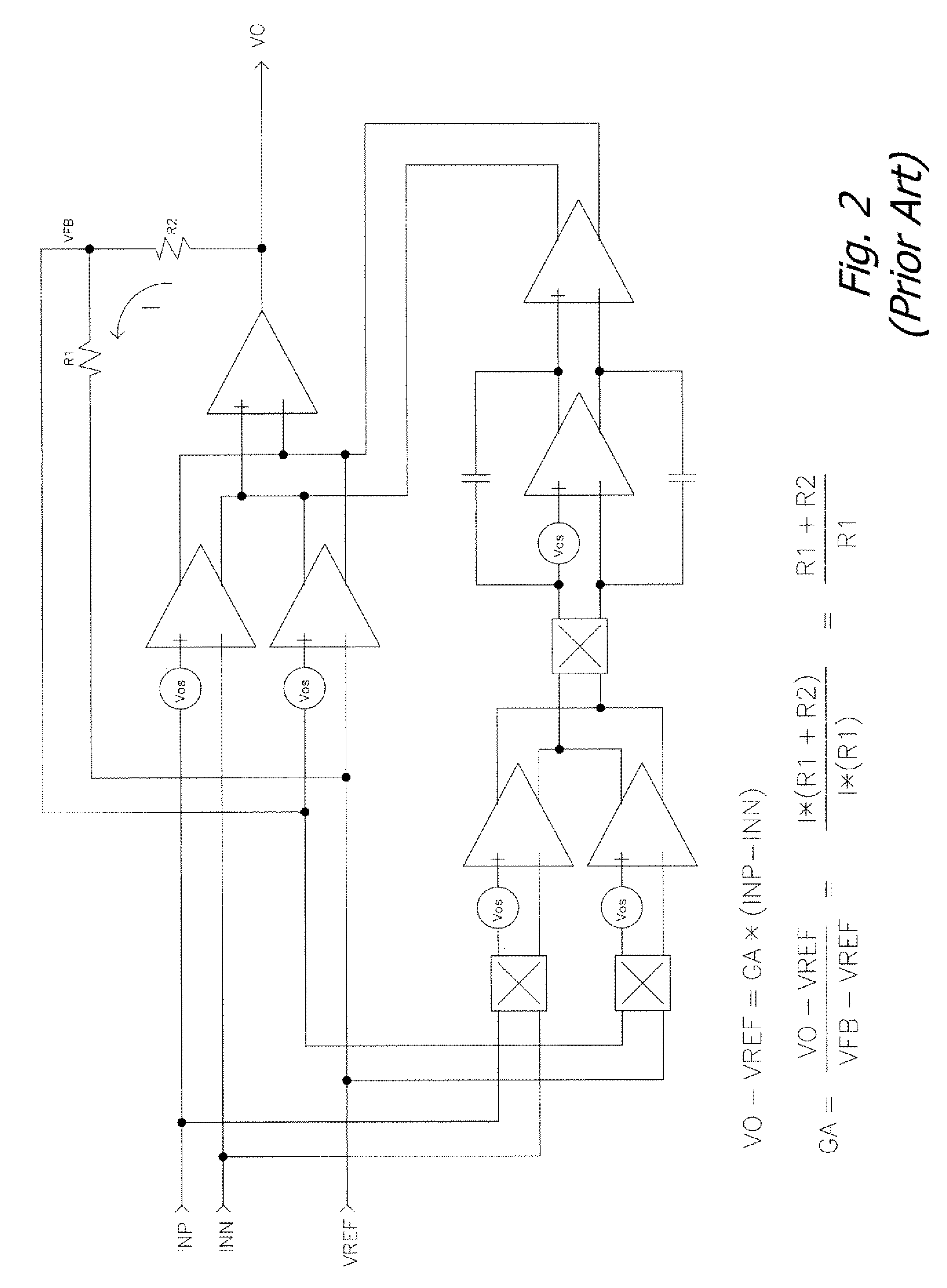
[0027]FIG. 3 illustrates the use of auto-zero techniques with input and feedback common mode voltage cancellation on the instrumentation amplifier between the choppers of FIG. 2. In FIG. 3, it is useful to illustrate the instrumentation amplifier as two distinct transconductance stages with outputs differenced (subtracted from one another). The objective of auto-zeroing is to effectively remove the offset of an amplifier by inserting series capacitors (CAZ) with the inverted offset voltage st...


PUM


Abstract

Auto-gain correction in a precision amplifier provides continuous calibration of the gain of the two differential input stages relative to each other and thus significantly minimizes the effects of device mismatch and temperature. Auto-gain correction together with auto-zero minimizes the effects of common mode input voltage on the amplifier and eliminates the need for trim associated with the matching of the two differential input stages. Improved gain matching enhances the accuracy of the auto-zero, which further improves the accuracy of auto-gain correction, resulting in a synergy with both operating together. The implementation of the auto-zero using an input pair of series capacitors in conjunction with a common input reference and a feedback pair of series capacitors in conjunction with a common feedback reference provides for decoupling the common mode voltage of the input differential pair or feedback differential pair. Various features may be used in sub-combinations as desired.

Description

BACKGROUND OF THE INVENTION[0001]1. Field of the Invention[0002]The present invention relates to the field of precision instrumentation amplifiers that provide high gain accuracy and low input offset.[0003]2. Prior Art[0004]The accuracy of the DC output of a linear amplifier is subject to the physical imperfections of the individual devices comprising the amplifier. The errors caused by the imperfections are Input-Offset (VOS) and Gain Error (GE). The amplifier output (VO) is the algebraic sum of the amplifier Input (VI) and Input-Offset times the amplifier Gain (GA). The Input-Offset of the amplifier is the input required for a zero output. In practice the amplifier input offset is determined from the output of the amplifier for a zero input divided by the gain of the amplifier.VO=GA*(VOS+VI)VO=GA*VOS for VI=0or VOS=VO / GA for VI=0[0005]Generally, an instrumentation amplifier has two differential input stages with low input bias currents. FIG. 1 shows one form of an instrumentation ...

Claims


Application Information

Patent Timeline
IPC IPC(8): H03F1/02
CPCH03F3/45475
Inventor BOUCHER, RICHARD EDWARDHUIJSING, JOHAN HENDRIK
Owner MAXIM INTEGRATED PROD INC
Why Eureka
Try Eureka