Substrate processing apparatus, substrate processing method, computer program, and storage medium

a substrate processing and substrate technology, applied in the direction of program control, instruments, packaged goods types, etc., can solve the problems of significant positional error or difference, /or deformation in each chamber, and errors in driving systems, etc., to avoid complicated configuration of placing tables, accurate assessment, and high accuracy

Active Publication Date: 2010-04-27
TOKYO ELECTRON LTD
View PDF6 Cites 26 Cited by
  • Summary
  • Abstract
  • Description
  • Claims
  • Application Information

AI Technical Summary

Benefits of technology

[0015]The present invention was made in light of the above circumstances, and therefore, it is an object of this invention to provide a substrate processing apparatus, a substrate processing method, and a computer program for use in the method, and a storage medium for storing the computer program, which can place a substrate in a correct position, even though some positional error occurs between the substrate carried in a processing vessel and a placing table. It is another object of this invention to provide a substrate processing apparatus, a substrate processing method, and a storage medium for storing a program for use in the method, which can take some necessary action at once against a positional error to be generated on a substrate, which has been detached from a placing table, after completion of a process.
[0037]According to the present invention, since the position of the substrate is optically detected by using the detecting head, in the transferring position above the transfer means, such as lifting pins, so as to correct the substrate transferring position based on the results of the detection, the substrate can be placed in a correct position on the placing table. Consequently, for example, in a plasma etching apparatus, trouble to be caused by the substrate which would ride on the focus ring and problems in the process to be associated with a positional error of the substrate can be avoided, and additionally more accurate assessment can be achieved for the results of processing the substrate. In addition, since the detecting head can be moved between the detection position and the evacuation position which is located outside the substrate transferring region, the outer periphery of the substrate can be detected with higher accuracy, and additionally complicated configuration of the placing table can be avoided. Furthermore, with the detecting head which can be completely housed in a wall portion of the processing vessel when it is in the evacuation position, for example, upon performing a process, the detecting head can be seen as a part of the wall face of the processing vessel. Thus, no trouble is caused, during the process, due to the provision of such a detecting head.
[0038]According to another aspect of the present invention, the substrate having been already processed is raised, by using the lifting pins, from the placing table, and the position of the substrate is optically detected by using the detecting head, so as to issue a warning based on the results of the detection. Thus, the operator can immediately take some necessary action, or the transferring position can be corrected automatically by the carrying apparatus, in response to the warning. As such, falling of the substrate from the carrying apparatus due to its collision with a transfer port of the processing vessel can be prevented. Additionally, the correction of the substrate transferring position based on the detection results can achieve a reliable substrate conveyance onto a correct position in a place to which the substrate is to be transferred.

Problems solved by technology

In the carrying apparatus, however, errors tend to occur in driving systems due to stretch or the like of driving belts provided in the carrying apparatus, and / or deformation is likely to occur in each chamber due to pressure to be applied to the large-sized carrying apparatus by the application of vacuum.
For example, in the case of carrying out processes, in succession, by carrying the wafer to one processing vessel after another in the multi-chamber system, since errors between the carrying apparatus and the wafer are accumulated, a significant positional error or difference may occur between the wafer transferring position for transferring the wafer from the carrying arm onto the lifting pins and the placing position of the placing table.
Therefore, if continuing such a mounting operation of the wafer while leaving the positional error as it is, the wafer may tend to ride on the focus ring surrounding the wafer placing position, thus making it difficult to perform a normal process, and the placing table which is not completely covered due to such a centered-off wafer may tend to be exposed to the plasma and thus damaged therewith.
In addition, such improper mounting of the wafer onto the placing position (i.e., the positional error between the respective central positions) may also lead to having negative impact on the yield of products.
Furthermore, in assessment on the process provided to the wafer, for example, in assessment on a profile of the etching rate in the surface of the wafer, factors to be attributed to the process parameters can not be distinguished from factors to be attributed to the aforementioned positional error of the wafer, as such making it difficult to analyze obtained data correctly and to carry out assessment accurately.
Moreover, because vacuum chuck can not be utilized in the vacuum processing apparatus, such as a plasma etching apparatus, as described above, the wafer is held by the placing table by using an electrostatic chuck utilizing coulomb force or Johnson-Rahbek force.
This is called de-chucking error.
Furthermore, if continuing operation of the carrying apparatus, irrespectively of occurrence of such a de-chucking error, failures of transfer of the wafer to the carrying apparatus and / or falling of the wafer from the carrying apparatus due to its collision with a transfer port of each processing vessel may occur.
Therefore, the shading area of the sensor light beam is significantly large, thus making it difficult to accurately measure fine differences.
In addition, a relatively long optical path of the sensor light renders adjustment of attaching positions of a light-emitting sensor and a light-receiving sensor significantly difficult.
Furthermore, deformation of the placing table to be caused by multiple exposure processes under high temperature conditions due to plasma may substantially shift the placing position of the wafer.
However, since the photo-sensor attached to the processing vessel is adapted to confirm only the wafer position, it can not be used to correct the positional error caused by factors on the side of the placing table.
Therefore, in some cases, the photo-sensor can not be completely covered with the wafer even after the wafer is placed on the placing table.
In such a case, a part of the photo-sensor, which is not covered with the wafer, is exposed to plasma, and is hence likely to be damaged.
Moreover, the placing table used in the plasma etching apparatus has a complicated structure because it includes an electrostatic chuck for fixing the wafer and a fluid passage for supplying a back side gas for enhancing heat conductivity between the placing face and the wafer rear face, in addition to the lifting pins described above.
Accordingly, these elements should make the structure of the placing table more complicated and thus impractical.

Method used


Image

  • Substrate processing apparatus, substrate processing method, computer program, and storage medium
  • Substrate processing apparatus, substrate processing method, computer program, and storage medium
  • Substrate processing apparatus, substrate processing method, computer program, and storage medium

Examples


examples

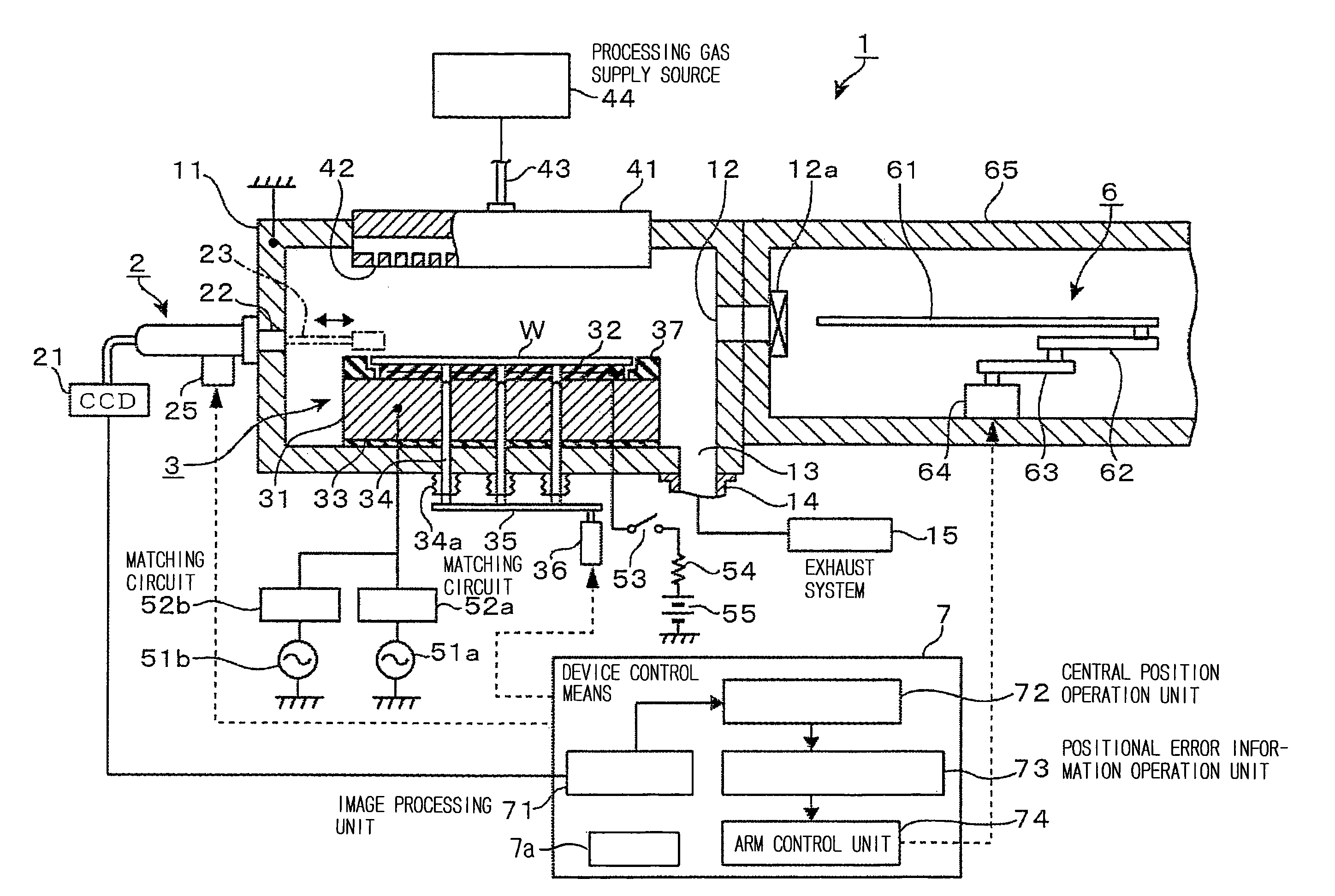
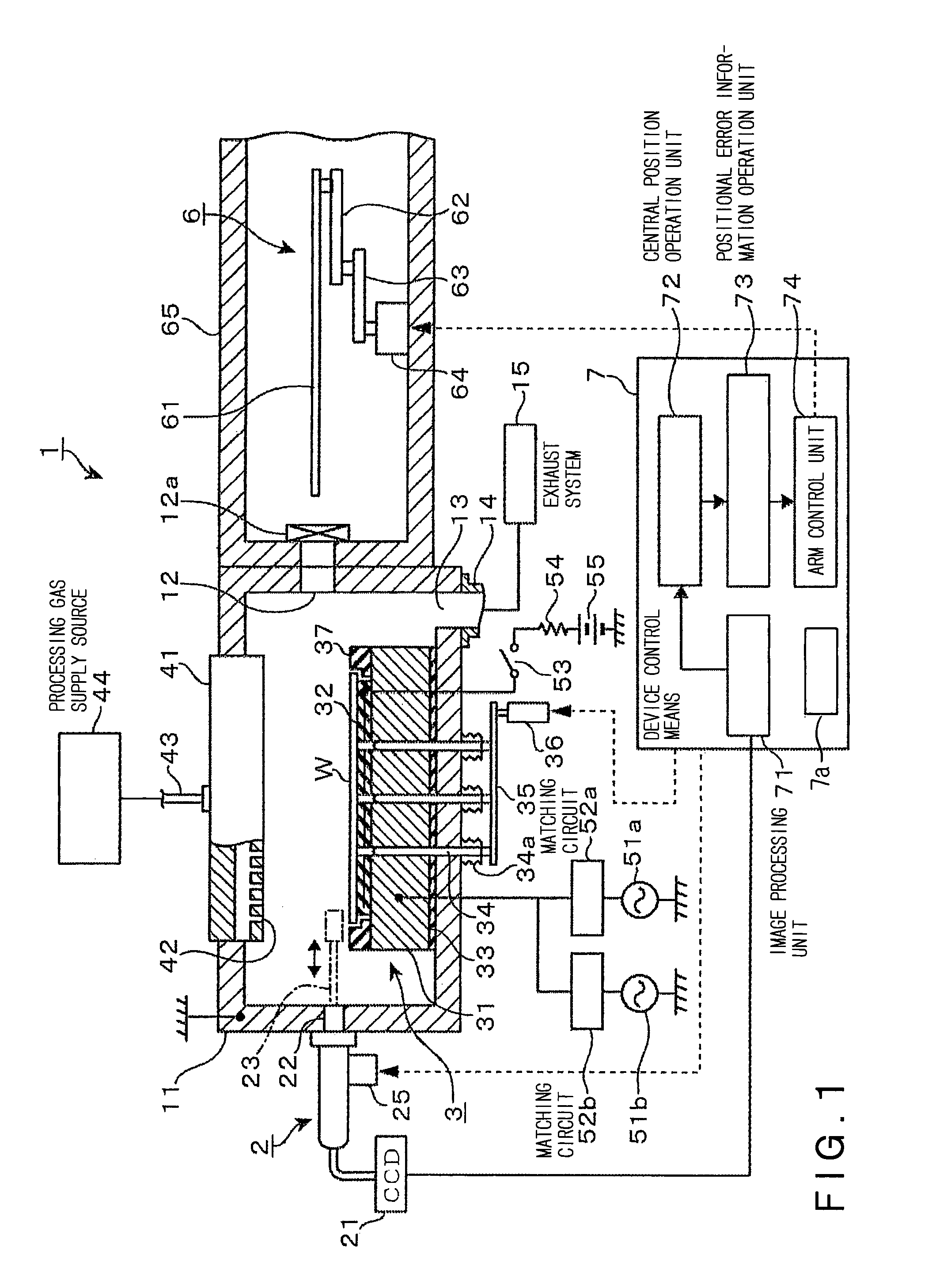
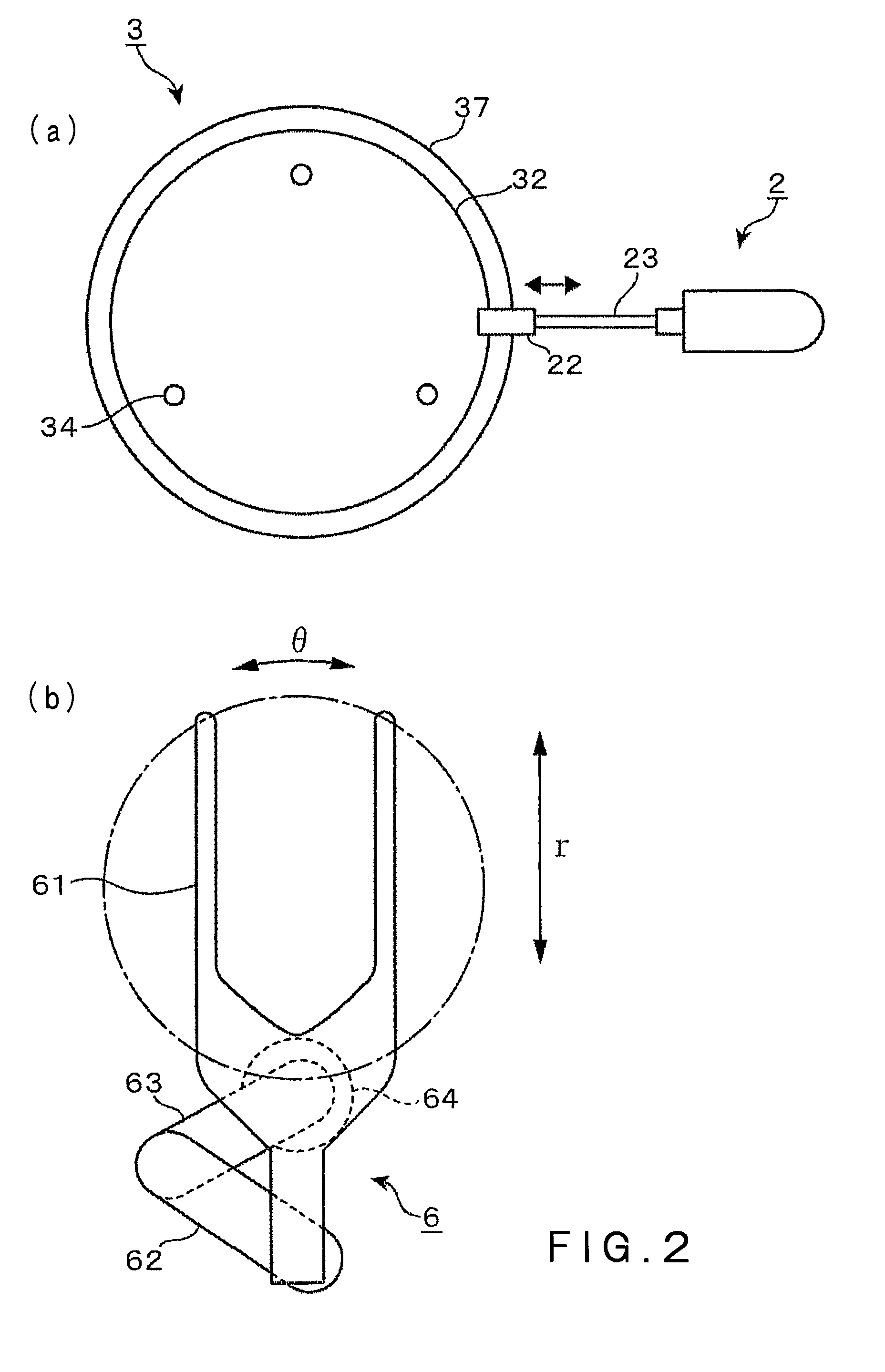
[0047]One embodiment, in which the present invention is applied to a plasma etching apparatus as a substrate processing apparatus, will be described below. FIG. 1 is one example of a plasma processing apparatus 1. The plasma processing apparatus 1 includes a processing vessel 11 formed of aluminum and used as, for example, a vacuum chamber, and a carrying apparatus 6 as a substrate carrying means, which is adapted to carry a wafer (substrate) W between the interior and the exterior of the processing vessel 11. In the interior of the processing vessel 11, a placing table 3 is provided to be located at a central position of a bottom wall of the processing vessel 11, and an upper electrode 41 is installed above the placing table 3 such that it is opposed to the placing table 3.

[0048]The processing vessel 11 has a contour of a generally rectangular parallelepiped shape, and an inner circumferential face of a circular shape, for example. In the bottom wall of the processing vessel 11, an...


PUM


Abstract

A substrate processing apparatus is provided, which can place a substrate in a correct position, even though a positional error occurs between the substrate carried in a processing vessel and a placing table. This substrate processing apparatus can take a necessary action immediately against a positional error of the substrate generated when the substrate is separated from the placing table after completion of a process. The plasma apparatus 1 includes a processing vessel 11, lifting pins 34 provided in the processing vessel 11, and a detecting head 22. A wafer W is carried into the processing vessel 11 from the exterior of the processing vessel 11 by using a carrying apparatus 6, and is stopped in a transferring position above the lifting pins 34. Thereafter, the detecting head 22 is moved from an evacuation position to a detection position, so as to obtain positional error information between a current position in which the wafer W is currently held and a programmed position in which the transfer of the wafer W is to be carried out. Based on the positional error information, the transferring position of the wafer W is corrected by using the carrying apparatus 6, such that an amount of the positional error between the current position W and the programmed position is within an allowable range.

Description

CROSS REFERENCE TO RELATED APPLICATIONS[0001]This application is based upon the prior Japanese Patent Application No. 2006-155275 filed on Jun. 2, 2006, the entire contents of which are incorporated herein by reference.BACKGROUND OF THE INVENTION[0002]1. Field of the Invention[0003]The present invention relates to a technique for detecting a position of a substrate and a technique for correcting the position of the substrate, in a processing vessel for providing a process, such as a plasma etching process and / or CVD process, to the substrate, for example, a semiconductor wafer.[0004]2. Background Art[0005]In a process for manufacturing a flat panel, such as a semiconductor device or liquid crystal display device, a substrate processing apparatus, such as a plasma etching apparatus or CVD apparatus, is used to provide a process, including etching and / or film forming, to a substrate, such as a semiconductor wafer (hereinafter, referred to as a wafer) or glass plate.[0006]Hereinafter, ...

Claims


Application Information

Patent Timeline
Patent Type & Authority Patents(United States)
IPC IPC(8): H01L21/68G06F19/00H01L21/205H01L21/3065H01L21/677
CPCH01L21/681
Inventor HIROKI, TSUTOMU
Owner TOKYO ELECTRON LTD
Why Eureka
Try Eureka