Component mounting apparatus and component mounting method

a technology of component mounting and component, which is applied in the direction of solventing apparatus, manufacturing tools, cooking vessels, etc., can solve the problem that the pump cannot be coated with the optimal amount of flux at the time of flux transfer, and achieve the effect of satisfactory adhesiveness and efficient component mounting

Inactive Publication Date: 2010-05-11
PANASONIC CORP
View PDF6 Cites 12 Cited by
  • Summary
  • Abstract
  • Description
  • Claims
  • Application Information

AI Technical Summary

Benefits of technology

[0006]Therefore, the present invention provides a component mounting apparatus and a component mounting method capable of simultaneously forming the coating films having different thicknesses and efficiently performing a component mounting with a satisfactory adhesiveness by ensuring the bump to be coated with the optimal amount of the paste.
[0009]Since the component mounting apparatus according to the present invention is configured such that the component mounting apparatus includes the paste transfer device which supplies the paste having at least two different thicknesses onto the bumps of a plurality of components held by the placement head, and the paste is applied to the bumps of the plurality of components in a bundle using the transfer coating method by lowering the plurality of components held by the placement head in the course of the movement of the placement head holding the plurality of components from the component supply unit to the circuit board holding unit,it is possible to form the coating films having different arbitrary thicknesses at the same time and ensure an optimal application amount of the paste, thereby efficiently performing the component mounting with a satisfactory adhesiveness.

Problems solved by technology

However, since the known paste transfer device including the above-mentioned example disclosed in Patent Document 1 cannot form coating films having arbitrarily different thicknesses at the same time, bumps cannot be coated with an optimal amount of the flux at the time of transferring the flux thereto.

Method used


Image

  • Component mounting apparatus and component mounting method
  • Component mounting apparatus and component mounting method
  • Component mounting apparatus and component mounting method

Examples


Embodiment Construction

[0022]Hereinafter, an embodiment of the invention will be described with reference to the drawings.

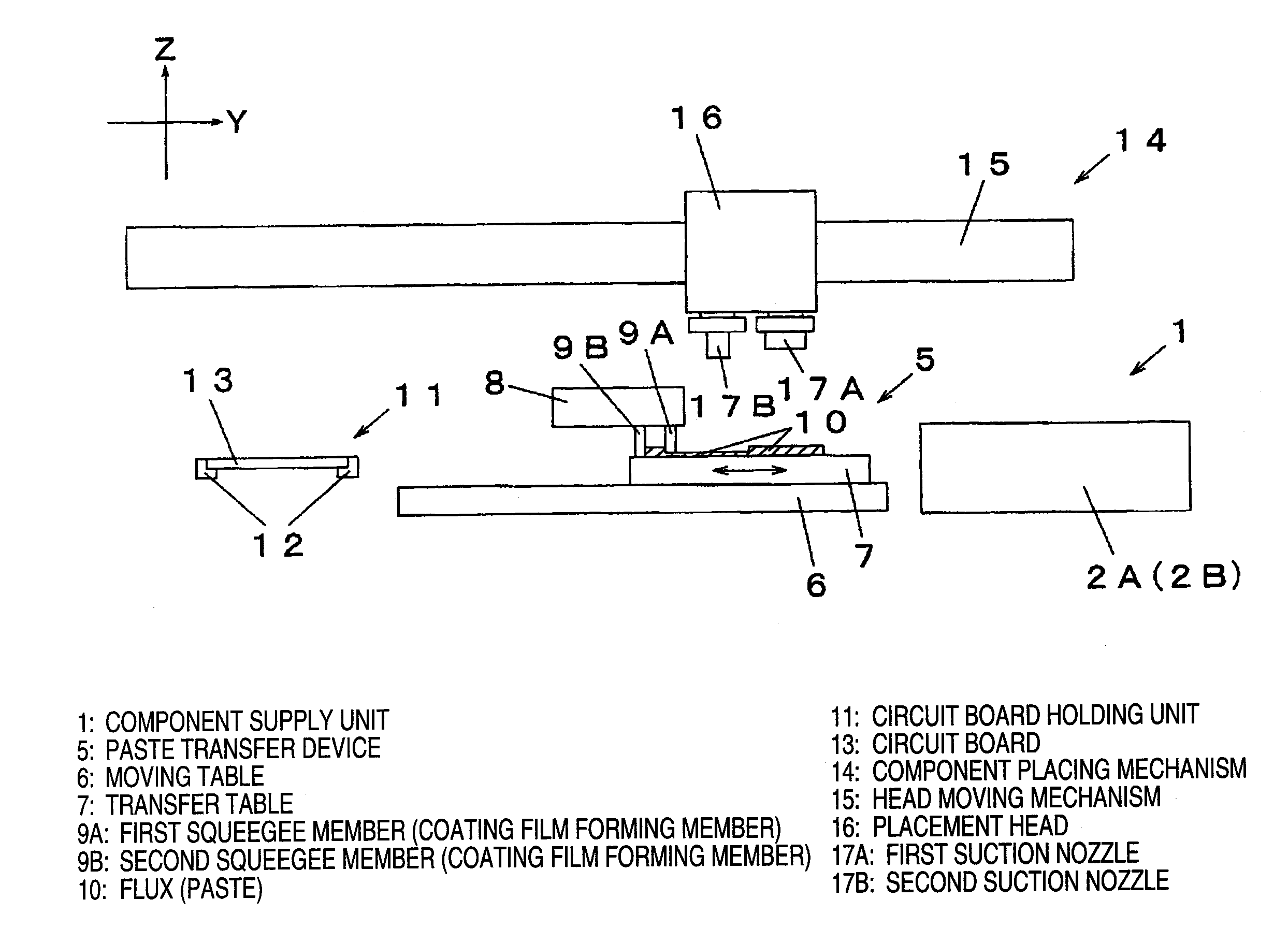
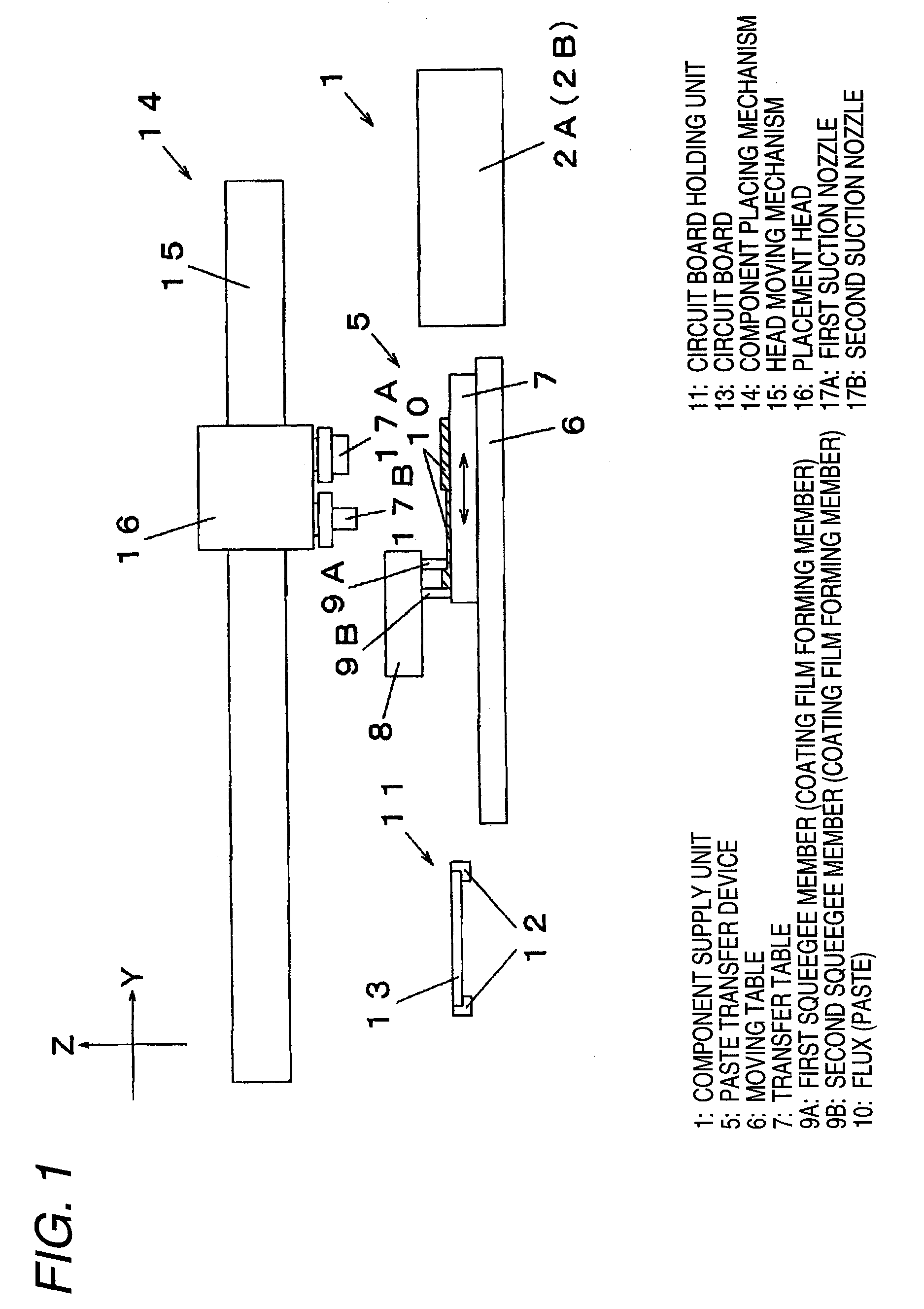
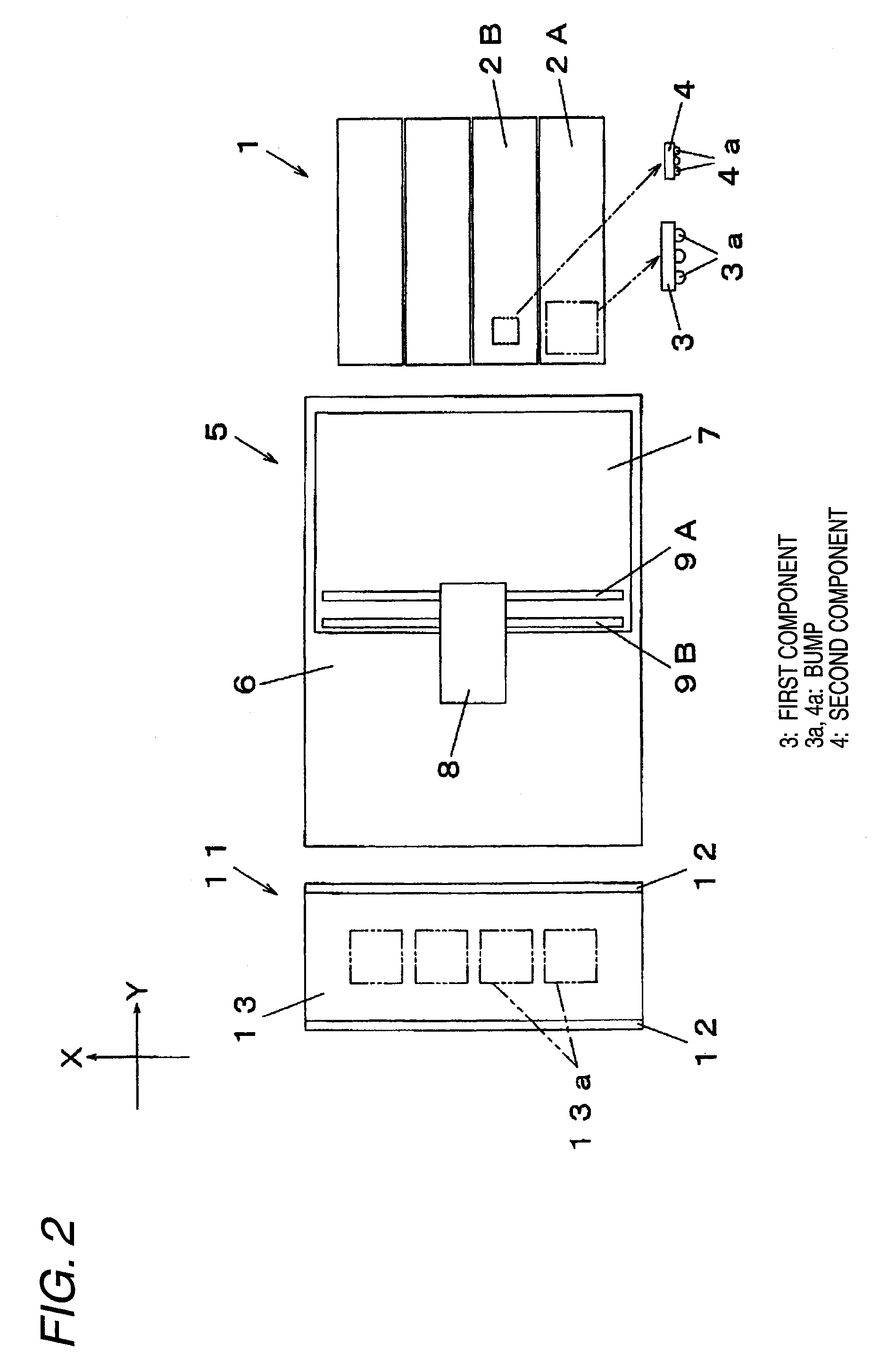
[0023]Moreover, a structure of the component mounting apparatus will be described with reference to FIGS. 1 and 2. The component mounting apparatus has a function of mounting components such as a semiconductor package in which a bump is formed on the lower surface thereof on a circuit board. As shown in FIGS. 1 and 2, the component mounting apparatus is configured that a component supply unit 1, a paste transfer device 5, and a circuit board holding unit 11 are two-dimensionally arranged in Y direction and a component placing mechanism 14 is disposed above them. In the specification, a circuit board conveying direction of the circuit board holding unit 11 is defined as X direction.

[0024]A plurality of components feeder including a first components feeder 2A and a second components feeder 2B are disposed in the component supply unit 1, and the first components feeder 2A and the second c...


PUM

PropertyMeasurementUnit
thicknessesaaaaaaaaaa
thicknessaaaaaaaaaa
adhesivenessaaaaaaaaaa

Abstract

First components and second components in which bumps are formed on the lower surface thereof and laminate structures are formed by mounting them to stack with each other on a circuit board 13 are picked up from a component supply unit 1 using a placement head 16, and by lifting and lowering the placement head 16 holding the first components and the second components relative to a paste transfer device 5 supplying a flux 10 in the manner such as coating films having two types of different thicknesses, the flux 10 is supplied to the bumps of the plurality of components in a bundle using a transfer coating method. With such a configuration, it is possible to efficiently perform a component mounting with a satisfactory adhesiveness by ensuring an optimal amount of application quantity of a paste.

Description

BACKGROUND OF THE INVENTION[0001]The present invention relates to a component mounting apparatus and method for mounting, on a circuit board, electronic components in which bumps are formed on the lower surface thereof.[0002]As a method of mounting electronic components such as semiconductor elements on a circuit board, there has been used a mounting method in which a semiconductor package having semiconductor elements mounted on a resin substrate is mounted on the circuit board by a solder bonding method using solder bumps. In the solder bonding method of bonding the electronic components onto the circuit board using the solder bumps, the bonding is generally conducted in such a manner that the solder bumps are landed onto electrodes formed on the circuit board in the state that an auxiliary substance for soldering such as a flux or a solder paste is supplied to the solder bumps. For this reason, a paste transfer device for transferring the flux or the solder paste is disposed in s...

Claims


Application Information

Patent Timeline
Patent Type & Authority Patents(United States)
IPC IPC(8): B23K31/00B23K31/02
CPCH01L24/81H01L24/95H01L25/0657H01L25/50H05K3/3484H05K3/3489H05K13/0465H01L24/743H01L24/75H01L24/13Y10T29/4913H01L2224/13099H01L2224/16145H01L2224/16225H01L2224/81024H01L2225/06513H01L2225/06517H01L2924/01002H01L2924/01033H05K2201/035H05K2201/10734H05K2203/0338H01L2924/01005H01L2924/01006H01L2924/01068H01L2924/01075H01L2924/014H01L2224/11822H01L2224/131Y10T29/53178Y10T29/53183H01L2224/81011H05K3/3485H05K13/04
Inventor MORITA, TAKESHIHIYOSHI, MASANORI
Owner PANASONIC CORP
Why Eureka
Try Eureka