
Mounting device for chips

a technology for mounting devices and chips, applied in semiconductor devices, lighting and heating apparatus, cooling/ventilation/heating modifications, etc., can solve the problems of high voltage use, unsteady use of conventional mounting devices, and high labor intensity of conventional mounting devices, and achieve the effect of cheap and easy installation

Inactive Publication Date: 2010-05-11
ACBEL POLYTECH INC
View PDF12 Cites 21 Cited by
  • Summary
  • Abstract
  • Description
  • Claims
  • Application Information

AI Technical Summary

Benefits of technology

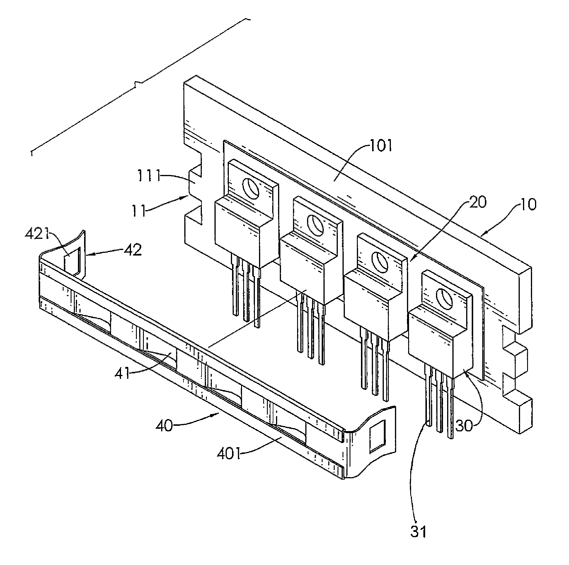
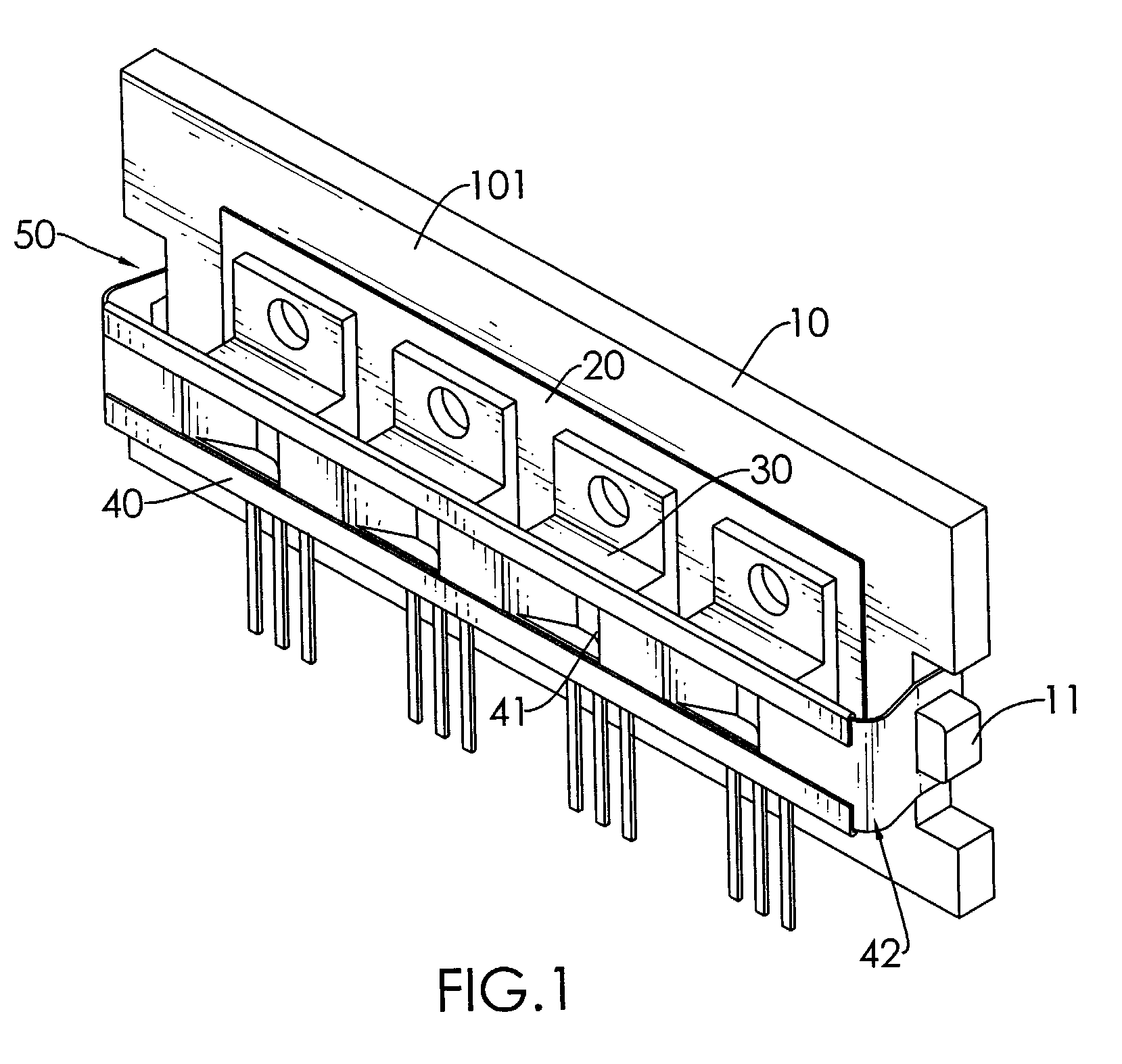
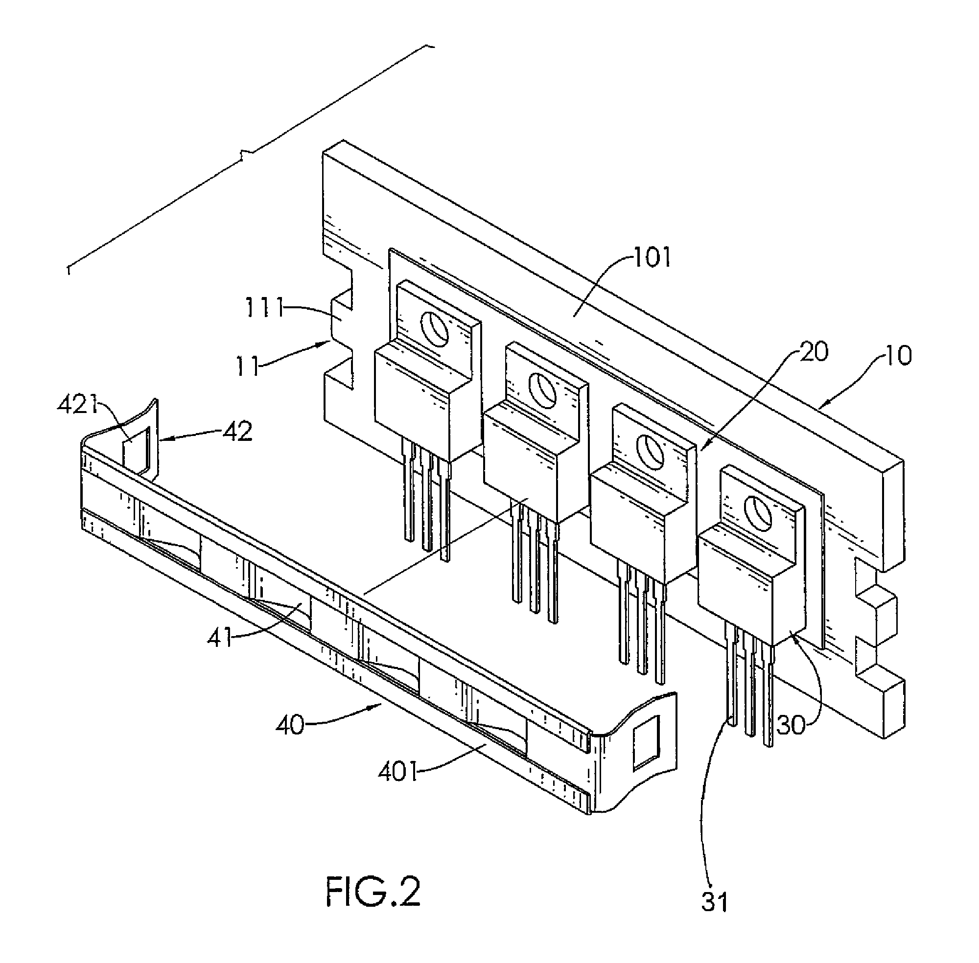
[0010]A mounting device for chips has a heat sink and at least one clamp. The heat sink has at least one conductive side, two ends, multiple chip units and two connecting bases. The chip units are arranged on the at least one conductive side. The connecting bases are formed on the ends of the heat sink. The at least one clamp is mounted across the at least one conductive side of the heat sink and has two ends, a middle sheet, multiple pressing tabs and two connecting arms. The pressing tabs extend from the middle sheet to press the chip units against the conductive side of the heat sink. The connecting arms are formed respectively on the ends of the clamp and are mounted respectively on the connecting bases. Consequently, the mounting device for chips provides a cheap and easy way to mount the chips on the conductive side of the heat sink at the same time.

Problems solved by technology

However, assembling the conventional mounting device takes a lot of time because components of the fastener (74) are small and tedious to install and connect.
Moreover, the conventional mounting device is unsteady when used with high voltage.
Because the chip unit (71) is so close to the bolt (741), voltage differential between the chip unit (71) and the bolt (741) is too high and may cause insulation breakdown or a flashover that will damage the chip unit (71).
This kind of mounting device is inconvenient and expensive to use in large volume applications because each clamping device (77) holds only one chip unit (71B).

Method used


Image

  • Mounting device for chips
  • Mounting device for chips
  • Mounting device for chips

Examples


Embodiment Construction

[0027]With reference to FIGS. 1, 4 and 6 to 12, a mounting device for chips in accordance with the present comprises a heat sink (10, 10A, 10B, 10C, 10D, 10E, 10F) and at least one clamp (40, 40A, 40B, 40C, 40D, 40E, 40F).

[0028]With further reference to FIG. 2, the heat sink (10, 10A, 10B, 10C, 10D, 10E, 10F) is a flat board, has at least one conductive side (101), two ends, at least one optional insulation spacer (20), multiple chip units (30), and two connecting bases (11, 11A, 11B, 11C, 11D, 11E, 11F).

[0029]The at least one insulation spacer (20) is attached to the at least one conductive side (101).

[0030]The chip units (30) are arranged longitudinally in a row and are attached on the at least one insulation spacer (20). Each chip unit (30) has multiple leads (31) extending transversely.

[0031]The connecting bases(11, 11A, 11B, 11C, 11D, 11E, 11F) are formed respectively on the ends of the heat sink (10, 10A, 10B, 10C, 10D, 10B, 10F). Each connecting base (11, 11A, 11B, 11C, 11D, ...


PUM


Abstract

A mounting device for chips has a heat sink and at least one clamp. The heat sink has at least one conductive side, two ends, multiple chip units and two connecting bases. The chip units are arranged on the at least one conductive side. The connecting bases are formed on the ends of the heat sink. The at least one clamp is mounted across the at least one conductive side of the heat sink and has two ends, a middle sheet, multiple pressing tabs and two connecting arms. The pressing tabs extend from the middle sheet to press the chip units against the conductive side of the heat sink. The connecting arms are formed respectively on the ends of the clamp and are mounted respectively on the connecting bases.

Description

BACKGROUND OF THE INVENTION[0001]1. Field of the Invention[0002]The present invention relates to a mounting device, and more particularly to a mounting device for chips, which incorporates a heat sink on which the chips are mounted.[0003]2. Description of the Prior Arts[0004]In the electronics industry, heat sinks are generally used on electronic components to dissipate heat generated by processing units. Many kinds of conventional mounting devices are used to mount chips on a heat sink.[0005]With reference to FIG. 13, a conventional mounting device for a chip in accordance with the prior art comprises a chip unit (71), an insulated gasket (72), a heat sink (73) and a fastener (74). The chip unit (71) comprises a chip and a mounting tab. The chip has a rear surface. The mounting tab is attached to and protrudes up from the rear surface of the chip and has an upper end, a rear surface and a mounting hole (711). The mounting hole (711) is formed through the mounting tab near the upper...

Claims


Application Information

Patent Timeline
Patent Type & Authority Patents(United States)
IPC IPC(8): H05K7/20F28F7/00H01L23/34
CPCH05K7/2049H01L23/367H01L23/4093H01L23/34
Inventor CHEN, JUNG-FATSAI, CHU-CHENG
Owner ACBEL POLYTECH INC
Learn More