Thin film having interpenetrating network layer and method for manufacturing the thin film
a technology of interpenetrating network layer and thin film, which is applied in the direction of transportation and packaging, synthetic resin layered products, organic chemistry, etc., can solve the problems of increasing the surface defect, increasing the risk of damage, etc., to achieve excellent durability and strength, excellent durability and strength lack flexibility, and self-supporting properties
- Summary
- Abstract
- Description
- Claims
- Application Information
AI Technical Summary
Benefits of technology
Problems solved by technology
Method used
Image
Examples
example 1
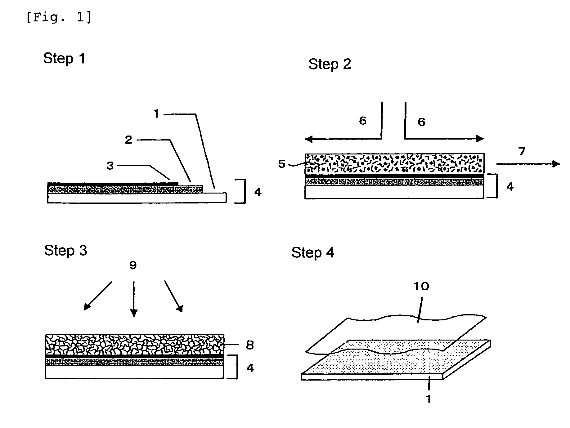
[0109]An IPN layer was configured according to the method shown in FIG. 1.
(Step (1))
[0110]A polyvinylphenol (PVPh) layer having a thickness of 100 nm was formed on a surface-treated silicon substrate (silicon wafer) (manufactured by Sumco Corporation) by a spin coating method. PVPh (manufactured by Aldrich) as used herein has a weight average molecular weight (Mw) of about 8,000 g / mole and high solubility in ethanol. Next, a polyvinyl alcohol (PVA) layer having a thickness of 5 nm was spin coated on the surface of the PVPh layer (layer thickness: 5 nm). PVA as used herein is one having been hydrolyzed in a proportion of 98% by mole and having a weight average molecular weight (Mw) of about 78,000 g / mole and is hydrophilic.
(Steps (2) to (3))
[0111]Next, a composition for IPN (A-1) prepared by dissolving 4-hydroxybutyl acrylate (manufactured by Acros Organics), hexanediol diacrylate (crossing agent) (manufactured by Alfa Aesar), zirconium tetrabutoxide (manufactured by Kanto Chemical C...
example 2
[0146]The same procedures as in Example 1 were followed, except for performing the Step (2) and Step (3) in an air atmosphere. As a result, it was confirmed that by performing the Step (3) in a nitrogen atmosphere, the polymerization more smoothly proceeded.
example 3
[0147]IPN thin films (B), (C) and (D) were manufactured in the same manner as in Example 1, except for changing the composition for IPN shown in Table 3 to prepare compositions for IPN (B), (C) and (D).
[0148]
TABLE 3CompositionPolymerizationfor IPNSi(NCO)4HOBuAHDODAinitiator(B)50.8 mol %46.8 mol %1.20 mol %1.19 mol %50.0 vol %46.9 vol %1.94 vol %1.19 vol %(C)67.4 mol %31.0 mol %0.79 mol %0.79 mol %66.7 vol %31.2 vol %1.29 vol %0.79 vol %(D)75.6 mol %23.2 mol %0.59 mol %0.59 mol %75.0 vol %23.4 vol %0.97 vol %0.59 vol %
[0149]In Table 3, Si(NCO)4, HOBuA and HDODA represent silicon tetraisocyanate, 4-hydroxybutyl acrylate and hexanediol diacrylate, respectively.
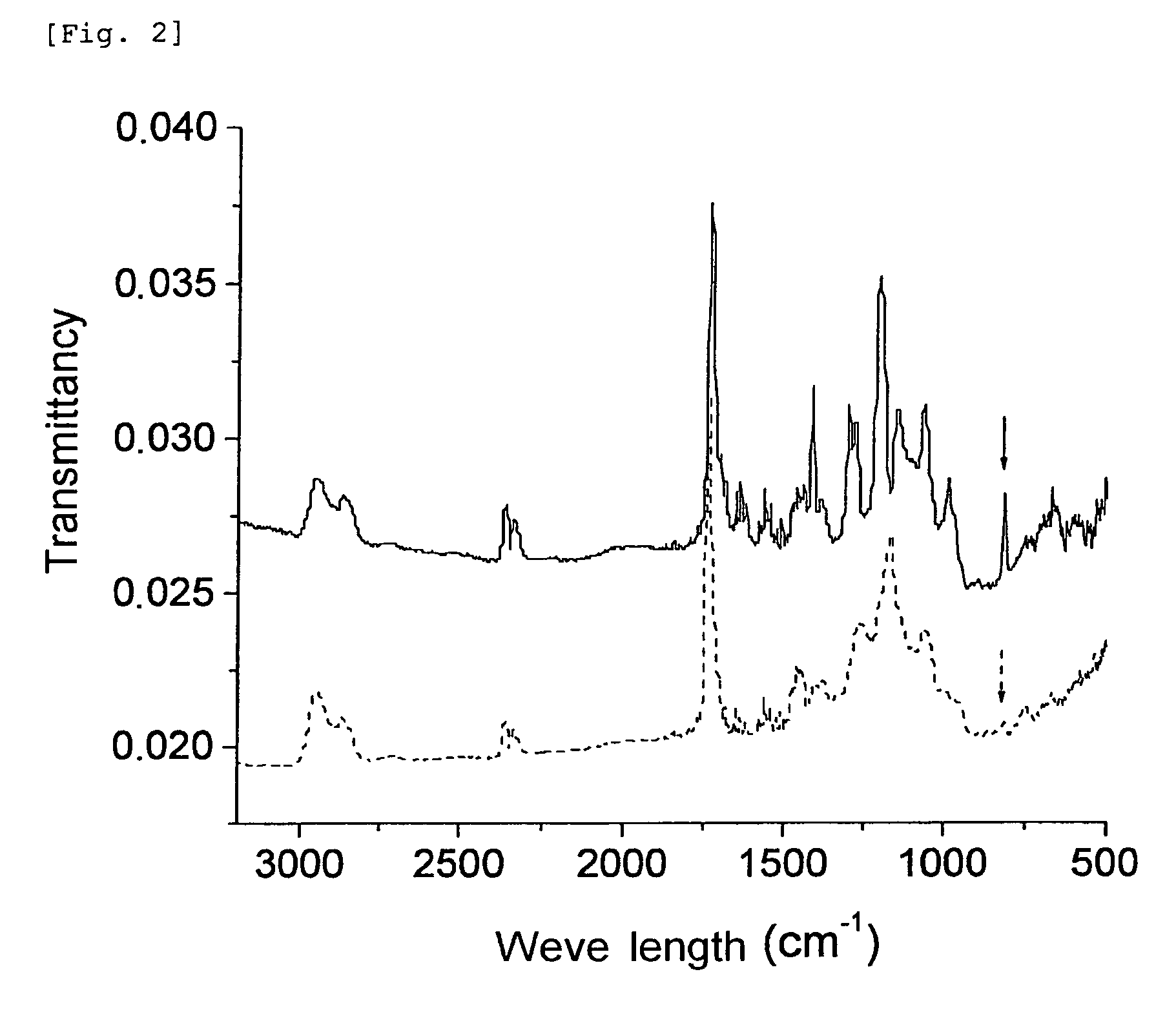
[0150]With respect to the obtained IPN thin films (B) to (D), an XPS spectrum was measured in the same manner as in Example 1. A composition of carbon, oxygen, nitrogen and silicon components obtained from the result is shown in Table 4.
[0151]
TABLE 4IPN thinfilmCarbonOxygenNitrogenSilicon(B)57.8 mol %32.9 mol % 1.9 mol %7.32 mol ...
PUM
| Property | Measurement | Unit |
|---|---|---|
| thickness | aaaaa | aaaaa |
| thickness | aaaaa | aaaaa |
| thickness | aaaaa | aaaaa |
Abstract
Description
Claims
Application Information


