Method and apparatus for de-jittering a clock signal

a clock signal and clock signal technology, applied in the field of signal transmission technique in electric technology, can solve the problems of more complexity, design of digitally controlled crystal oscillators, and difficult implementation, and achieve the effects of low cost, easy implementation, and easy implementation

Active Publication Date: 2010-05-25
HUAWEI TECH CO LTD
View PDF15 Cites 7 Cited by
  • Summary
  • Abstract
  • Description
  • Claims
  • Application Information

AI Technical Summary

Benefits of technology

[0015]It can be seen from FIG. 4 that feedback circuit of this jitter attenuator is pretty simple, so the system structure thereof is simpler than that of the first jitter attenuator shown in FIG. 3, but still difficult to implement, especially design of the digitally controlled crystal oscillator. Hereby, the output of crystal oscillator can be taken as a source of de-jittered clock, so that the de-jittered clock is of very high quality. However, the disadvantages are more complexity and less flexibility. The digitally controlled crystal oscillator is complicated to design and the output frequency range is restricted because of the limited pull-in range of the crystal. Multilevel analogue operational amplifiers and large dimension of the load capacity further increase the cost of this scheme. Besides, this de-jittering method cannot implement the transition between T1 clock frequency and E1 clock frequency either, thus cannot meet the practical requirements under certain circumstances.
[0016]Therefore, the present invention is to provide a de-jittering method for a clock signal, which can make structure of the de-jittering circuit for E1 or T1 signals simpler and further implement transition between T1 clock frequency and E1 clock frequency, so as to meet practical requirements better.
[0017]The present invention also is to provide a de-jittering apparatus for a clock signal, which is of simpler structure and can further implement transition between T1 clock frequency and E1 clock frequency, so as to meet practical requirements better.
[0059]Preferably, the controllable divider is a digital frequency synthesizer or other devices that can perform frequency division according to the control signal. It can be seen from the above technique scheme that, in the de-jittering method for the clock signal, the digital phase-locked loop is constituted by adopting the controllable divider and basic principle of digital phase-locked loop is used, the control signal of the controllable divider is generated by comparing the clock signal to be de-jittered as the reference signal and the feedback clock signal outputted by the controllable divider, so that the stable clock signal outputted by the controllable divider can be adjusted and controlled, the stable clock signal is outputted as the feedback clock signal and the clock signal to be de-jittered. Therefore, principle of this method is simple and it is easy to implement.
[0060]The de-jittering apparatus for the clock signal includes a control-signal generating circuit and a controllable divider, which is of distinct structure and easy implementation. The apparatus bears the advantages of low cost and high reliability because of very little area occupied in the integrated circuit.
[0061]In addition, because the control-signal generating circuit generates the control signal according to a signal that is to be de-jittered, it can control multiple controllable dividers to output different de-jittered clock signals. If two controllable dividers are adopted, when only one T1 or E1 clock signal to be de-jittered is inputted, two de-jittered clock signals, namely a T1 signal and an E1 signal, can be outputted, so that transition between T1 clock signal frequency and E1 clock signal frequency can be implemented to meet practical requirements better.

Problems solved by technology

It can be seen from FIG. 4 that feedback circuit of this jitter attenuator is pretty simple, so the system structure thereof is simpler than that of the first jitter attenuator shown in FIG. 3, but still difficult to implement, especially design of the digitally controlled crystal oscillator.
However, the disadvantages are more complexity and less flexibility.
The digitally controlled crystal oscillator is complicated to design and the output frequency range is restricted because of the limited pull-in range of the crystal.
Multilevel analogue operational amplifiers and large dimension of the load capacity further increase the cost of this scheme.
Besides, this de-jittering method cannot implement the transition between T1 clock frequency and E1 clock frequency either, thus cannot meet the practical requirements under certain circumstances.

Method used


Image

  • Method and apparatus for de-jittering a clock signal
  • Method and apparatus for de-jittering a clock signal
  • Method and apparatus for de-jittering a clock signal

Examples


Embodiment Construction

[0071]To make technical scheme and advantages of the present invention more distinct and understandable, the present invention will be described hereinafter with reference to the accompanying drawings and two preferable embodiments.

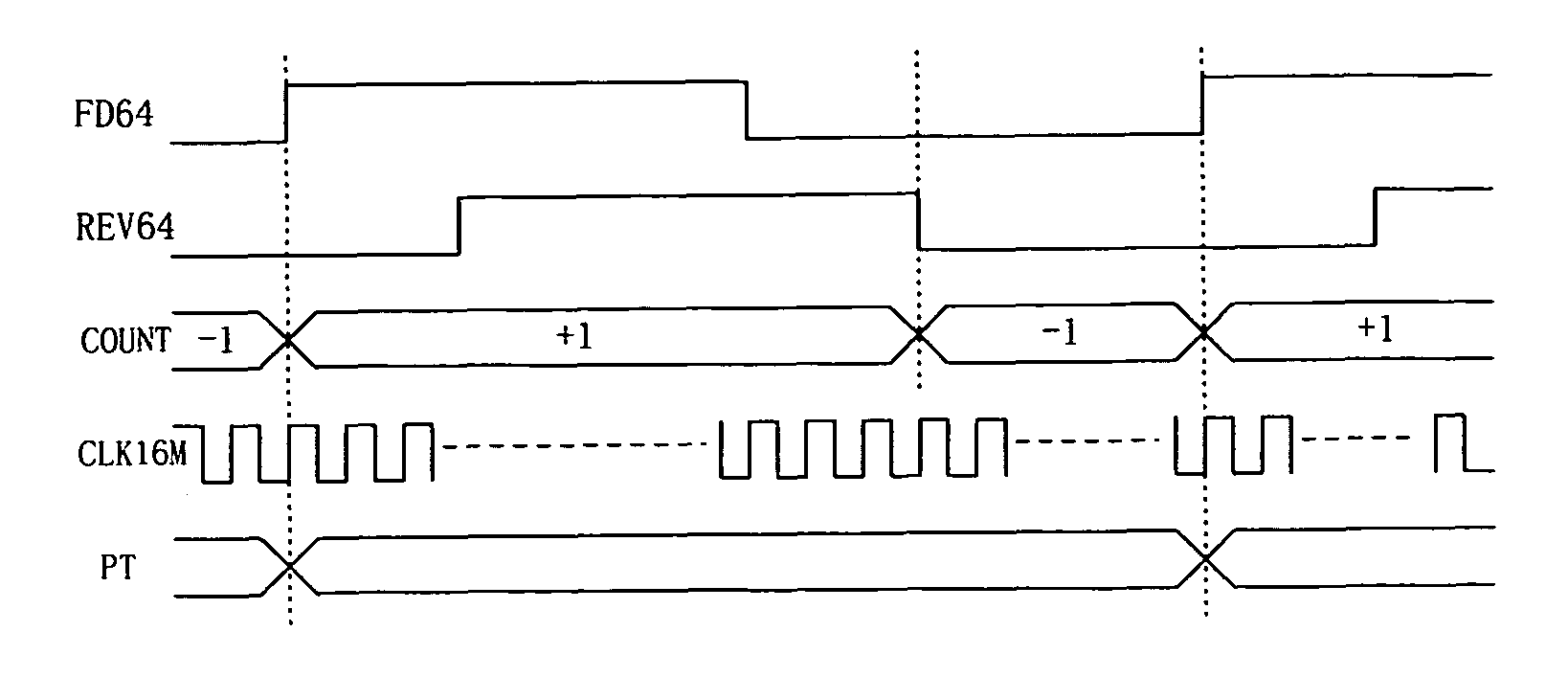
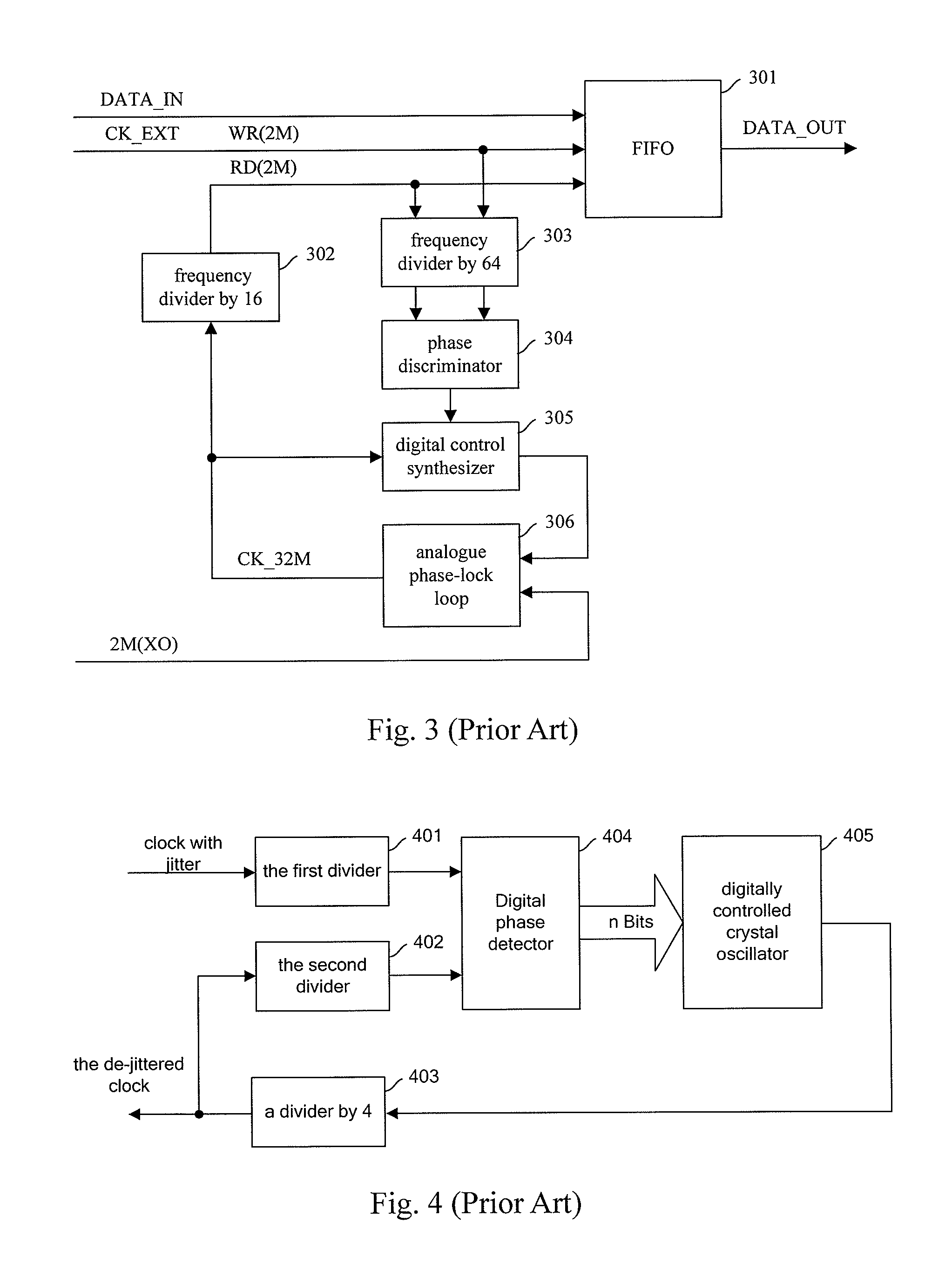
[0072]The de-jittering method and apparatus for the clock signal in the embodiment adopts controllable dividers to constitute a digital phase-locked loop, and uses the basic principle of digital phase-locked loop to attenuate jitter of the clock signal, wherein the de-jittering procedure includes:

[0073]A. taking the clock signal to be de-jittered as a reference signal, and comparing it with a feedback clock signal outputted by a controllable divider;

[0074]B. generating a control signal according to the comparison result and outputting the control signal to the controllable divider;

[0075]C. the controllable divider dividing the input high-frequency signal to generate a stable clock signal according to this control signal, and outputting the stable clock si...


PUM


Abstract

The present invention discloses a de-jittering method for a clock signal, which is implemented by adopting a controllable frequency divider and includes: taking the clock signal to be de-jittered as a reference signal, and comparing a feedback clock signal outputted by the controllable frequency divider with the reference signal; generating the control signal that is then transmitted to the controllable frequency divider; the controllable frequency divider performs frequency division upon the input high-frequency signal to generate a stable clock, and the stable clock is outputted as the feedback clock signal which has been de-jittered. The present invention also discloses a de-jittering apparatus for implementing the above-mentioned method, which includes: a circuit for generating a control signal and a controllable frequency divider. By applying the present invention, the de-jittering circuit for clock signal can be simple. What's more, transition between T1 clock frequency and E1 clock frequency can also be implemented to meet practical requirements better.

Description

[0001]This application is a continuation of International Patent Application No. PCT / CN2005 / 000652, filed on May 10, 2005, which claims priority to Chinese Patent Application No. 200410044467.2, filed on May 10, 2004, all of which are hereby incorporated by reference.FIELD OF THE TECHNOLOGY[0002]The present invention relates to signal transmission technique in electric technology field, more particularly to a de-jittering method and apparatus for a clock signal.BACKGROUND OF THE INVENTION[0003]In order to make a communication system operate normally, the system's clock and data must meet certain jitter requirements. Therefore, some communication equipments must be equipped with a jitter-attenuating function to wipe off the signal jitter generated during the communication, so as to guarantee accuracy and reliability of the signal reception. Accordingly, a series of international standards and protocols have been presented to regulate de-jittering standards. At present, jitter attenua...

Claims


Application Information

Patent Timeline
Patent Type & Authority Patents(United States)
IPC IPC(8): H04B3/46H03L7/08H04J3/06
CPCH03L7/08H04J3/0626
Inventor XIA, JUN
Owner HUAWEI TECH CO LTD
Why Eureka
Try Eureka