Photoelectric conversion film laminated color solid-state imaging apparatus

a technology of photoelectric conversion and color solid-state imaging, which is applied in the direction of television system scanning details, radioation control devices, television systems, etc., can solve the problems of reducing light use efficiency, single color signal for each pixel, and reducing sensitivity, so as to prevent degradation of linearity of photoelectric conversion characteristics and high sensitivity

Inactive Publication Date: 2010-06-01
FUJIFILM CORP
View PDF11 Cites 2 Cited by
  • Summary
  • Abstract
  • Description
  • Claims
  • Application Information

AI Technical Summary

Benefits of technology

[0020]A second object of the invention is to provide hybrid type photoelectric conversion film laminated color solid-state imaging apparatus having a CMOS type signal read circuit that improves color separation between red color (R) and blue color (B) to obtain good color reproducibility.
[0045]With this configuration, a potential barrier region that behaves as a potential barrier to the signal charges of pixels composed of a photoelectric conversion film. This keeps constant the terminal voltage of the photoelectric conversion film irrespective of the amount of accumulated signal charge, thus preventing degradation of linearity of the photoelectric conversion characteristic as well as loss of color balance. Further, color reproducibility is enhanced through color separation using a color filter.

Problems solved by technology

This worsens light use efficiency and lowers sensitivity.
Another problem is that only a single color signal is obtained for each pixel.
Thus, the resulting resolution drops and false colors appear conspicuous.
The problem is that this type of imaging apparatus is difficult to manufacture and the corresponding manufacturing yield is low, which results in a higher cost.
Thus, separation of the spectrum response characteristic of R signal, G signal and B signal is not sufficient enough and the resulting color reproducibility is low.
As a result, the proportional relationship between the light intensity and the output signal is lost and the linearity of the photoelectric conversion characteristic is degraded.
Thus, in the hybrid type imaging apparatus, it is difficult to strike a balance between the red light and blue light detected by the photodiode and the green light detected by the photoelectric conversion film, which results in a lower picture quality.
Because the light incident on each photodiode contains no G light, color separation between R and B is improved although color separation is not good enough as far as the difference of the light absorption coefficient of a semiconductor substrate is used.
For example, red light incident on a photodiode for blue color generates an optical charge thus failing to obtain acceptable color reproducibility.

Method used


Image

  • Photoelectric conversion film laminated color solid-state imaging apparatus
  • Photoelectric conversion film laminated color solid-state imaging apparatus
  • Photoelectric conversion film laminated color solid-state imaging apparatus

Examples


first embodiment

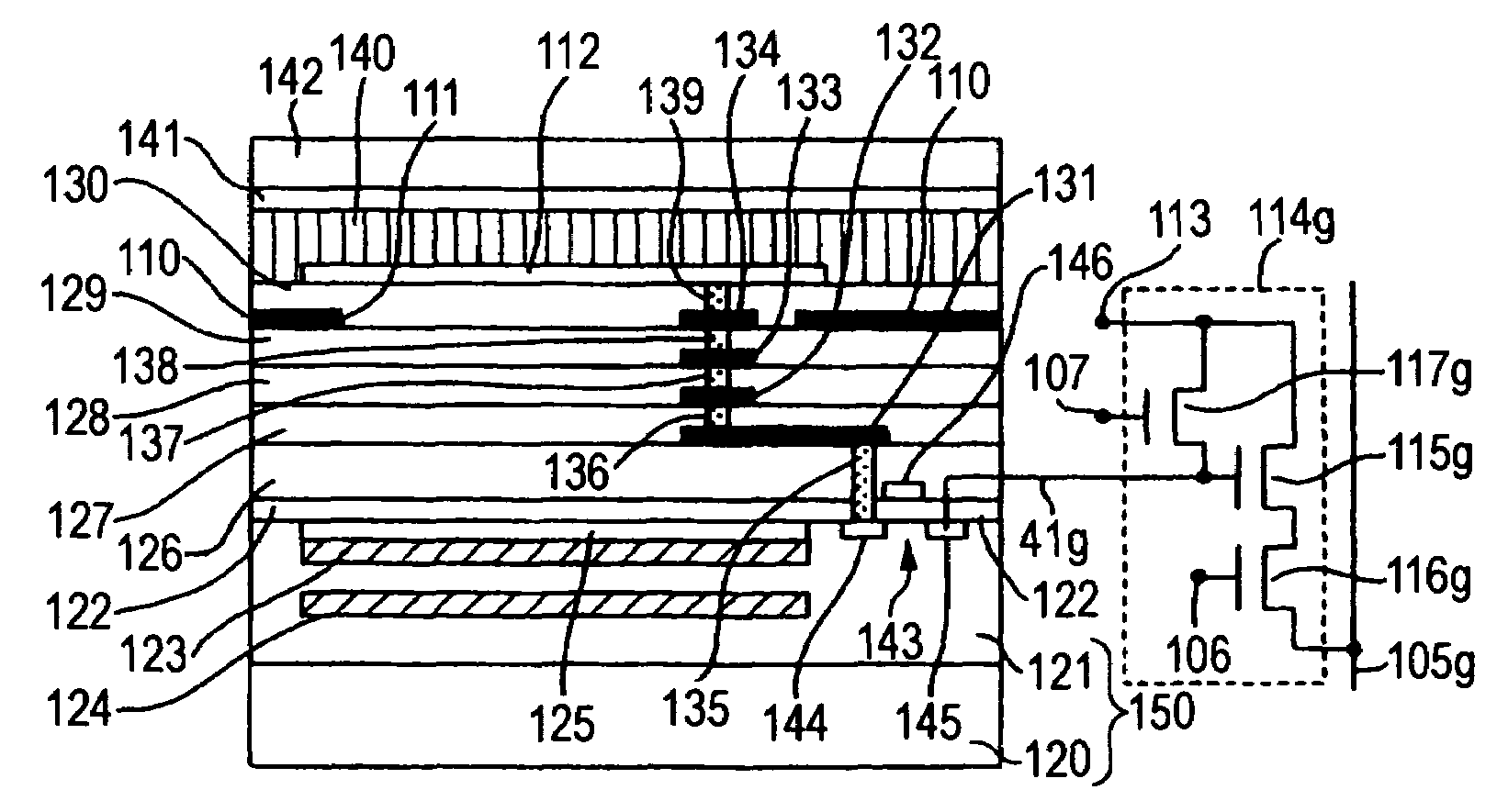
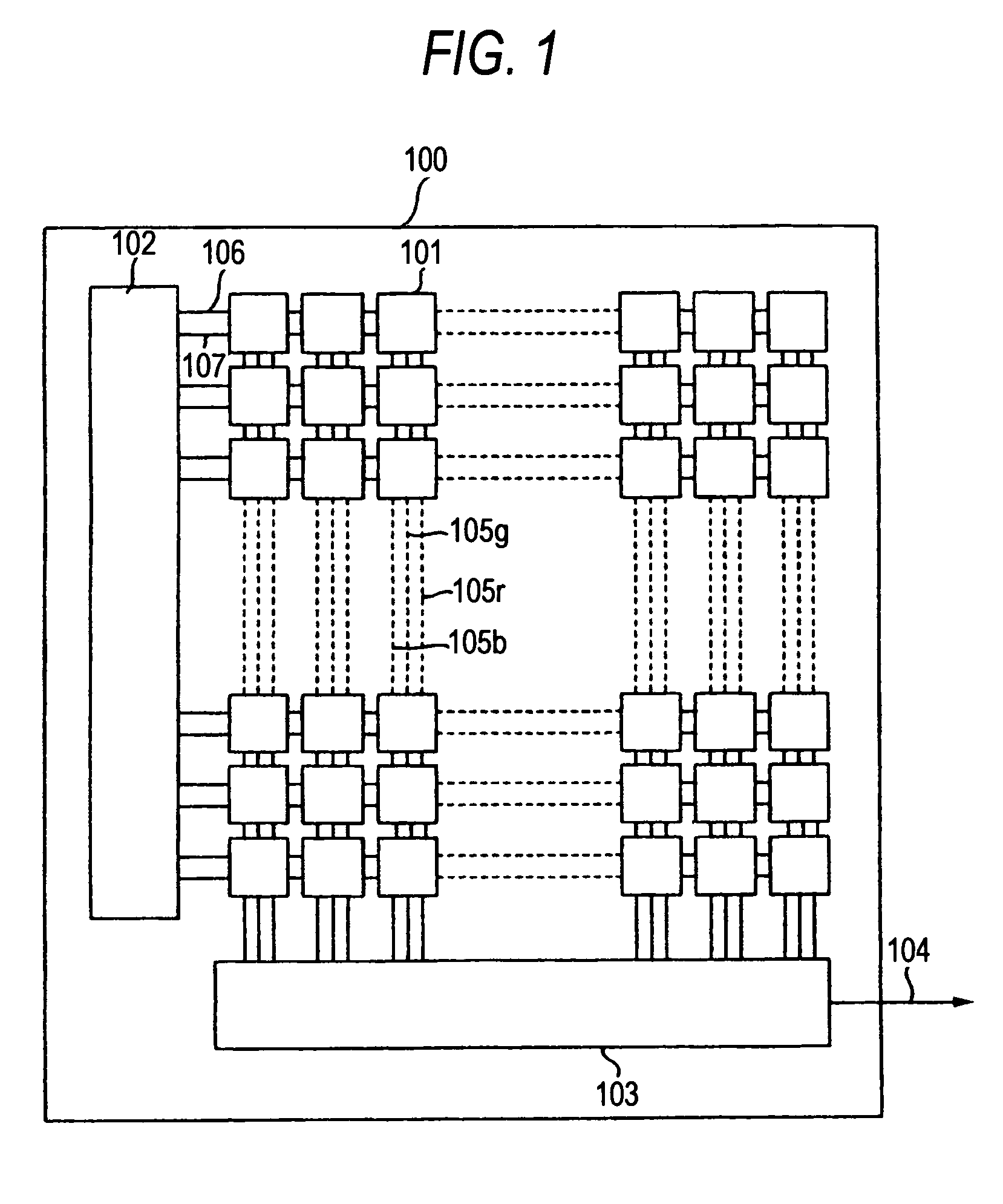
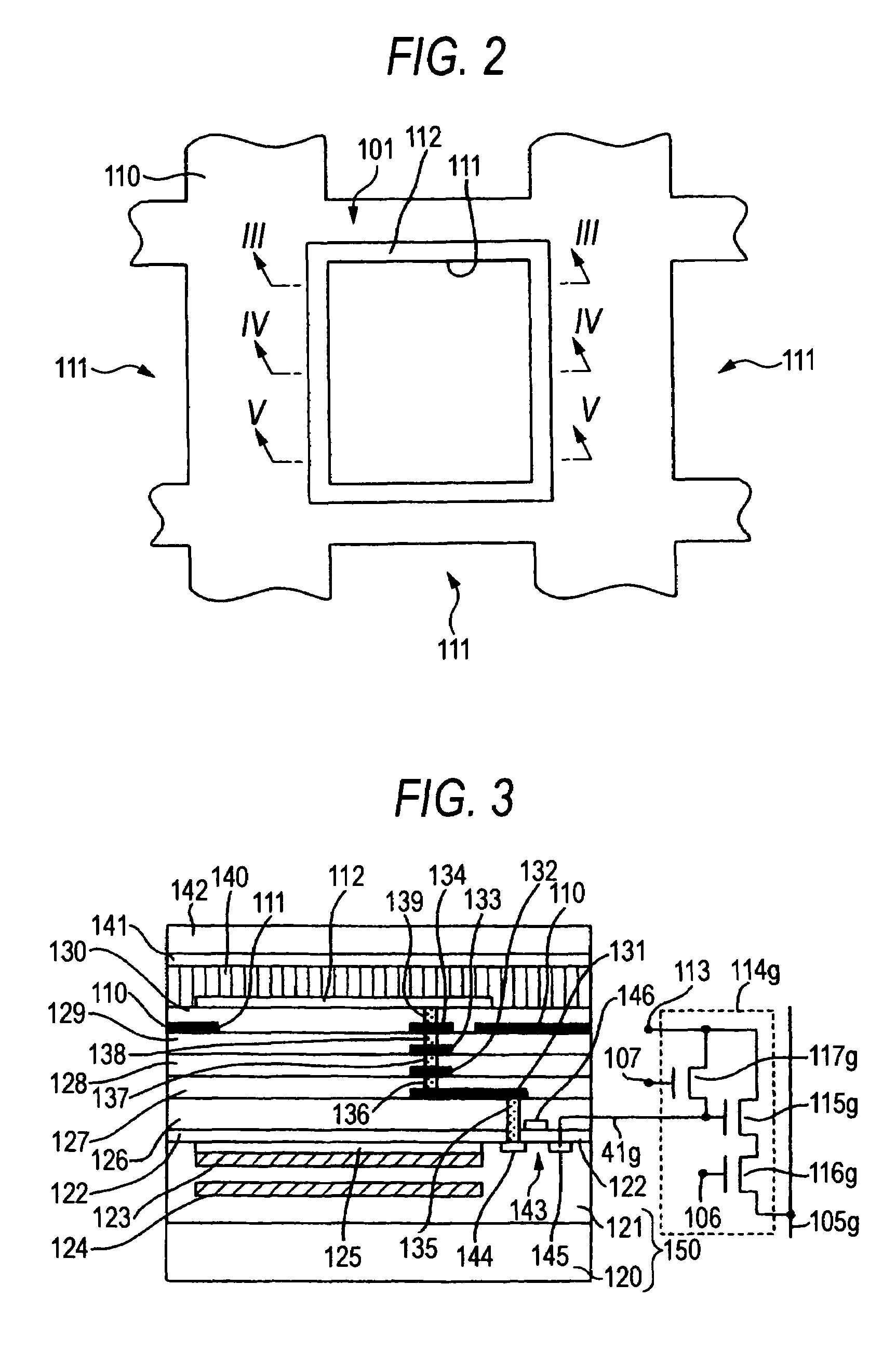
[0060]FIG. 1 is a surface schematic view of photoelectric conversion film laminated color solid-state imaging apparatus according to the first embodiment of the invention. The photoelectric conversion film laminated color solid-state imaging apparatus 100 includes a large number of light receiving parts 101 in a tetragonal lattice in this example. On the surface of a semiconductor substrate of the photoelectric conversion film laminated color solid-state imaging apparatus 100 are formed a photodiode for detecting blue light and a photodiode for detecting red light mentioned later as well as a signal read circuit composed of a MOS transistor circuit by using a circuit integration technique. In the upper layer of the semiconductor substrate are laminated a photoelectric conversion film by way of a film forming technique.

[0061]Three signal read circuits provided for the light receiving parts 101 are interconnected via a row selection scan circuit 102, a row selection signal line 106 an...

second embodiment

[0092]FIG. 6 is a surface schematic view of photoelectric conversion film laminated color solid-state imaging apparatus 200 according to the second embodiment of the invention. The photoelectric conversion film laminated color solid-state imaging apparatus 200 differs from the photoelectric conversion film laminated color solid-state imaging apparatus 100 according to the first embodiment of the invention shown in FIG. 1 in that a read signal line 208 connecting a signal read circuit for each light receiving part 101 to a row selection scan part 102 is added.

[0093]FIGS. 7, 8 and 9 are respectively schematic cross-sectional views of the imaging apparatus according to this embodiment corresponding to FIGS. 3, 4 and 5 according to the first embodiment. A same sign is given to a same member as the first embodiment and the corresponding description is omitted.

[0094]In this embodiment, a potential barrier part 251b of a separate structure is provided in place of the potential barrier tran...

third embodiment

[0102]FIG. 10 is a surface schematic view of photoelectric conversion film laminated color solid-state imaging apparatus according to the third embodiment of the invention. While two n-type semiconductor layers 123, 124 are provided in the direction of depth of the semiconductor substrate and a blue color signal and a red color signal are separately detected by taking advantage of the wavelength dependency of the distance of entry of light in the first embodiment shown in FIG. 1, a color filter is used to separate a red color signal from a blue color signal to enhance the color separation performance, same as the related art practices. A red filter is formed at a light receiving part 101 bearing “R” in FIG. 1 and a blue filter is formed at a light receiving part 101 bearing “B”.

[0103]In this embodiment, a single light receiving part 101 is used to detect two colors of green and blue, and another light receiving part 101 adjacent thereto is used to detect two colors of green and red....


PUM


Abstract

A photoelectric conversion film laminated color solid-state imaging apparatus comprising: a semiconductor substrate in which a first signal read circuit for a first color among the three primary colors, a second signal read circuit for a second color and a third signal read circuit for a third color are formed by MOS transistor circuits, and in which first and second photodiodes for respectively receiving incident light of the first and second colors are formed; a photoelectric conversion film provided above the semiconductor substrate, for receiving incident light of the third color to generate an optical charge; a longitudinal wiring for connecting a pixel electrode film attached to the photoelectric conversion film separately for each pixel to a contact part formed in the semiconductor substrate; and a potential barrier part between the contact part and the third signal read circuit, being formed on the semiconductor substrate.

Description

BACKGROUND OF THE INVENTION[0001]1. Filed of the Invention[0002]The present invention relates to photoelectric conversion film laminated color solid-state imaging apparatus that receives the incident light of one color among the three primary colors with photoelectric conversion films laminated on a semiconductor substrate and receives the incident light of the remaining two colors transmitted by the photoelectric conversion film with a photoelectric conversion device formed on the semiconductor substrate, and in particular to photoelectric conversion film laminated color solid-state imaging apparatus that provides good color balance between a color signal obtained from the light received with the photoelectric conversion film and that obtained from the light received with the photoelectric conversion device.[0003]2. Description of the Related Art[0004]Single board type color solid-state imaging apparatus represented by a CCD type or CMOS type image sensor arranges in a mosaic three...

Claims


Application Information

Patent Timeline
Patent Type & Authority Patents(United States)
IPC IPC(8): H04N3/14H01L27/146H01L31/10
CPCH04N5/335H04N25/00
Inventor SUZUKI, NOBUO
Owner FUJIFILM CORP
Why Eureka
Try Eureka