Image sensor

a technology of image sensor and image, applied in the field of image sensor, can solve the problem that the image sensor may output an image with and achieve the effect of suppressing the production of periodical fixed pattern noise and improving the readout speed

Active Publication Date: 2010-06-01
CANON KK
View PDF38 Cites 14 Cited by
  • Summary
  • Abstract
  • Description
  • Claims
  • Application Information

AI Technical Summary

Benefits of technology

[0010]It is an object of the present invention to, e.g., improve the readout speed in a mode in which one pixel signal is read out from each target readout area and suppress production of periodical fixed pattern noise on an image to be output from an image sensor in this mode.
[0021]According to the present invention, it is possible to, e.g., improve the readout speed in a mode in which one pixel signal is read out from each target readout area and suppress production of periodical fixed pattern noise on an image to be output from an image sensor in this mode.

Problems solved by technology

However, Japanese Patent Laid-Open No. 2005-286933 does not describe any idea of increasing the frame rate used in capturing a moving image from that in capturing a still image.
However, Japanese Patent Laid-Open No. 2005-130382 does not describe any concept of parallely outputting sums through a plurality of channels.
Since the circuit arrangements for reading out pixels with a low resolution are arrayed periodically in the image sensor, the image sensor may output an image having periodical fixed pattern noise.

Method used


Image

  • Image sensor
  • Image sensor
  • Image sensor

Examples


first embodiment

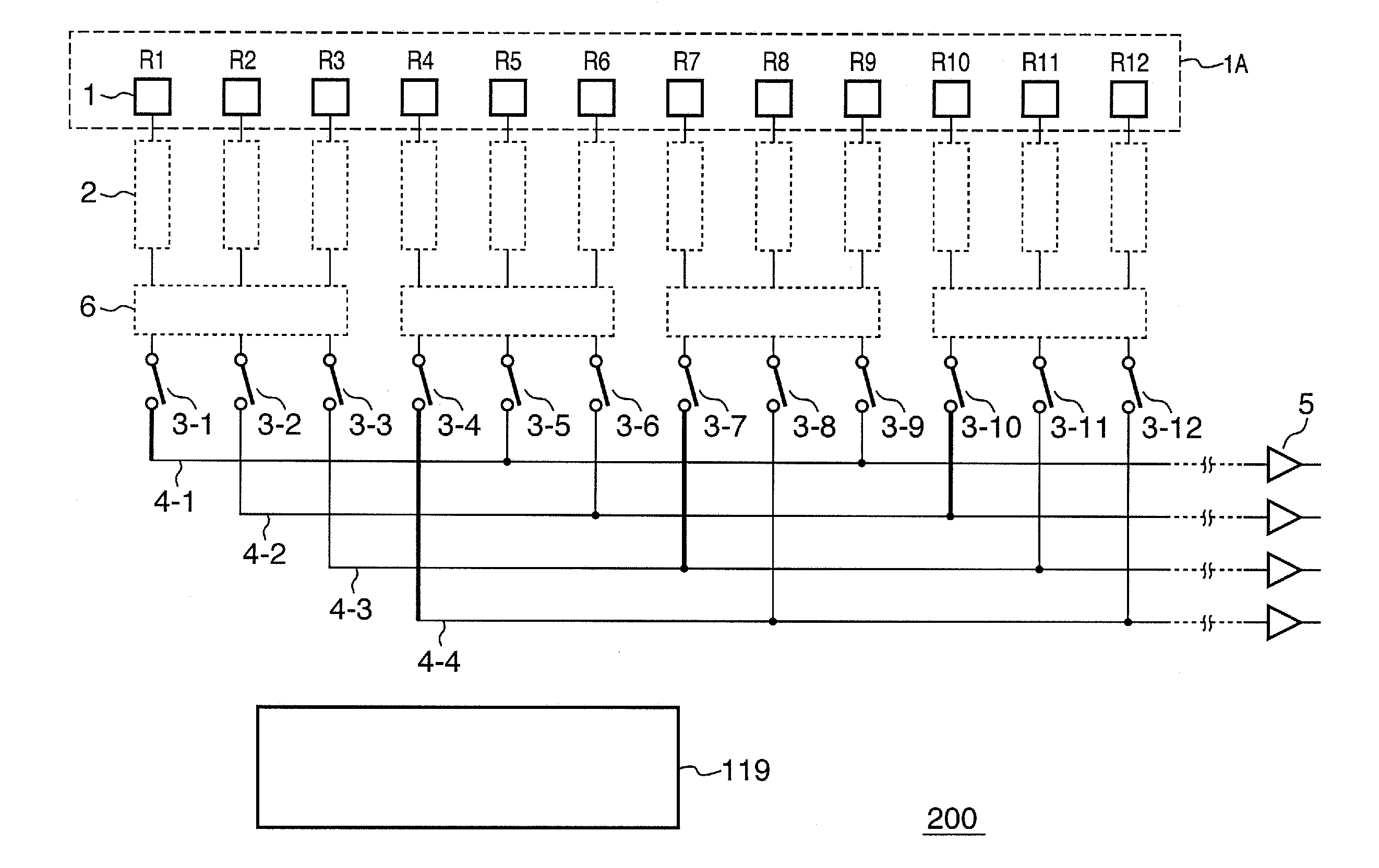
[0037]FIG. 1 is a circuit diagram showing the schematic arrangement of an image sensor according to the first embodiment of the present invention. An image sensor 200 provides a full pixel readout mode (second readout mode) in which the pixel signals of all pixels are read out, and a low resolution readout mode (first readout mode) in which one pixel signal is read out from each target readout area. The average readout mode will be exemplified below as the low resolution readout mode. The average readout mode here indicates a mode in which the average value of pixel signals of a plurality of pixels included in a target readout area is read out.

[0038]The image sensor 200 comprises a pixel array area 1A where a plurality of pixels 1 is arrayed. In the pixel array area 1A, the pixels 1 can be arranged to form a plurality of columns or one or a plurality of rows. FIG. 1 shows only pixels R1 to R12 of one row corresponding to a red filter. Each readout circuit 2 generates a pixel signal ...

second embodiment

[0063]FIG. 7 is a circuit diagram showing the schematic arrangement of an image sensor according to the second embodiment of the present invention. Color filters R, Gr, Gb, and B in the Bayer array are formed on pixels 100, and an area sensor is built by two-dimensionally arraying picture elements each of 2×2 pixels.

[0064]FIG. 8 is an equivalent circuit diagram of the pixel 100. A transfer pulse PTX, i.e., PTX1, PTX2, . . . controls a transfer switch 102. A reset pulse PRES, i.e., PRES1, PRES2, . . . controls a reset switch 103. A row selecting pulse PSEL, i.e., PSEL1, PSEL2, . . . controls a row selecting switch 105. A vertical scanning circuit 123 generates the transfer pulse PTX, reset pulse PRES, and row selecting pulse PSEL.

[0065]A full pixel readout operation in an image sensor 300 shown in FIG. 7 will be explained with reference to the timing chart of FIG. 9. The following description assumes that a set exposure time has elapsed and a photodiode 101 accumulates photocharges p...

third embodiment

[0074]FIG. 12 is a block diagram showing the schematic arrangement of an image sensor according to a preferred embodiment of the present invention. A camera 400 comprises a solid-state image sensor 1004 exemplifying image sensors according to the first and second embodiments.

[0075]A lens 1002 forms an optical image of an object on the image capturing plane of the image sensor 1004. The outer surface of the lens 1002 is covered with a barrier 1001 which protects the lens 1002 and also serves as a main switch. The lens 1002 has a stop 1003 to adjust the quantity of light passing through the lens 1002. An image capturing signal processing circuit 1005 performs various processes such as correction and clamping for image capturing signals output from the image sensor 1004 through a plurality of channels. An A / D converter 1006 performs analog-to-digital conversion of image capturing signals output from the image capturing signal processing circuit 1005 through a plurality of channels. A s...


PUM


Abstract

An image sensor includes a plurality of operation circuits. The operation circuit operates pixel signals read out from a group of pixels included in a readout area to generate a pixel signal in the thinning readout mode. A plurality of column selecting switches are arranged between the output terminals of the plurality of operation circuits and a plurality of output channels. A control circuit controls the plurality of column selecting switches such that pixel signals the number of which is equal to the number of the plurality of output channels are output to the plurality of output channels in parallel in the thinning readout mode. The circuit arrangements, each included in the corresponding one of the plurality of operation circuits and each viewed from the corresponding one of the column selecting switches used in the thinning readout mode, are equivalent to each other.

Description

BACKGROUND OF THE INVENTION[0001]1. Field of the Invention[0002]The present invention relates to an image sensor.[0003]2. Description of the Related Art[0004]These days, image sensors for digital cameras make remarkable progress and are rapidly gaining a larger number of pixels for higher resolution of still images. Along with this, it is an urgent issue to increase the pixel signal readout speed in order to ensure sequential shooting performance necessary for a camera. Japanese Patent Laid-Open No. 2005-286933 discloses a CCD image sensor which parallely reads out pixel signals through a plurality of column shift registers to increase the readout speed.[0005]A digital camera can capture still images and even moving images. The digital camera generally uses one image sensor to capture both still and moving images. The image sensor requires high resolution for still images, and requires a high frame rate for moving images while decreasing the resolution to match a general moving imag...

Claims


Application Information

Patent Timeline
Patent Type & Authority Patents(United States)
IPC IPC(8): H04N5/335H04N5/341H04N5/345H04N5/347H04N5/365H04N5/374H04N5/378
CPCH04N3/1568H04N5/335H04N5/23245H04N23/667H04N25/46H04N25/75H04N25/00
Inventor HIYAMA, HIROKITAKADA, HIDEAKIHATANO, YUICHIROARISHIMA, YU
Owner CANON KK
Why Eureka
Try Eureka