Systems and methods for issuing address and data signals to a memory array
a memory array and address signal technology, applied in the field of semiconductor memory, can solve the problems of insufficient storage, failure of traditional method of ensuring write and system clock synchronization by delaying the write clock signal to match the system clock signal delay, and unable to know how much storage would be needed
- Summary
- Abstract
- Description
- Claims
- Application Information
AI Technical Summary
Benefits of technology
Problems solved by technology
Method used
Image


Examples
Embodiment Construction
[0017]Certain details are set forth below to provide a sufficient understanding of embodiments of the invention. However, it will be clear to one skilled in the art that embodiments of the invention may be practiced without various of these particular details. In some instances, well-known circuits, control signals, and timing protocols have not been shown in detail in order to avoid unnecessarily obscuring the described embodiments of the invention.
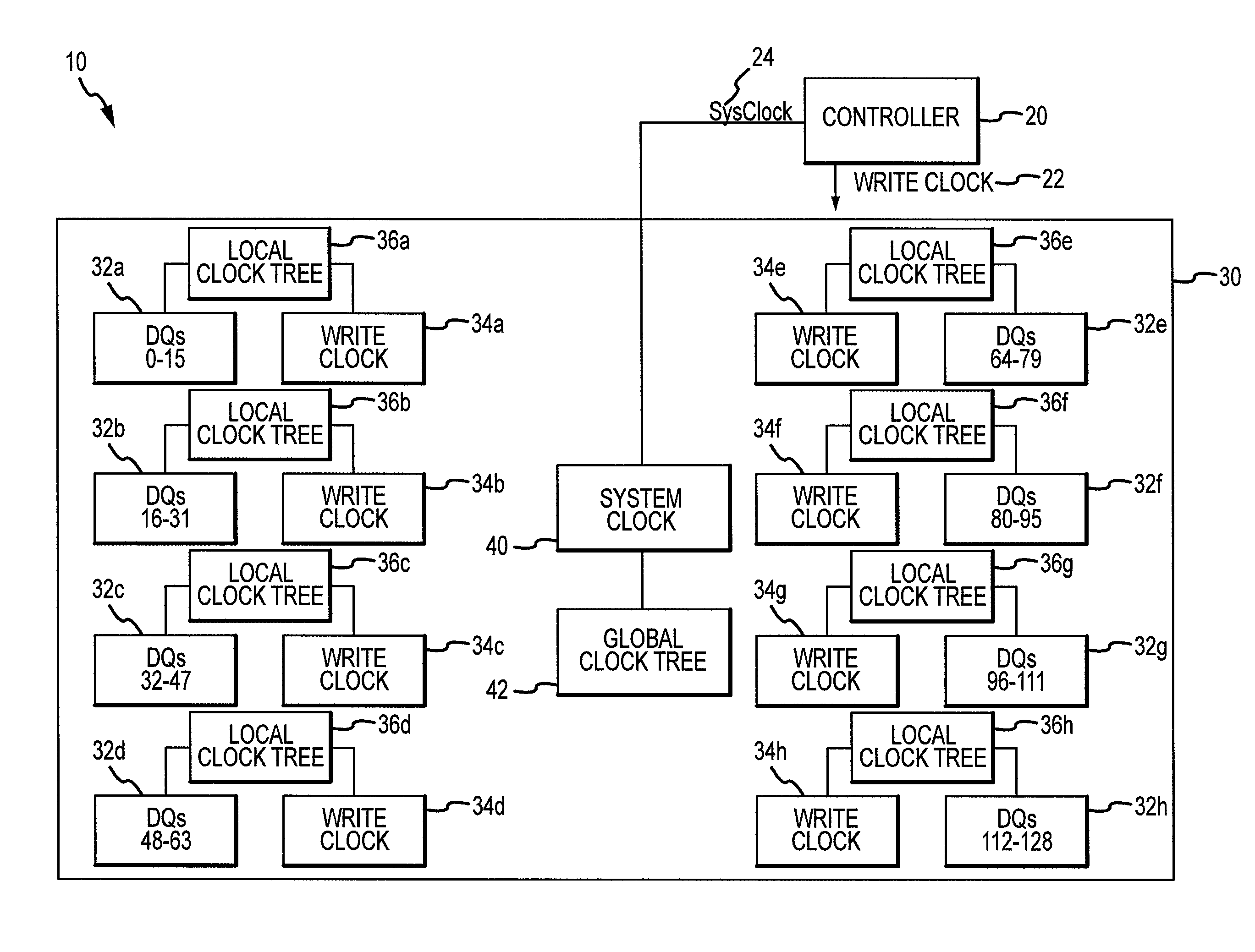
[0018]FIG. 2 depicts an embodiment of circuitry 100 for issuing data and address signals to a memory array for a memory access operation according to an embodiment of the present invention. A write clock signal 22, write data signal 105, and system clock signal 24 are generally in synch when provided to the circuitry 100. The write clock signal 22 is provided to a local clock tree 110, which in turn provides a write clock signal 22′ to a data capture latch 115. The write data signal 105 is routed through a local clock tree mock delay 112...
PUM
 Abstract
Description
Claims
Application Information