Semiconductor device having a through electrode with a low resistance and method of manufacturing the same

a technology of through electrode and semiconductor device, which is applied in the direction of semiconductor device, semiconductor/solid-state device details, electrical apparatus, etc., can solve the problems of reducing the operating speed, reducing the voltage, and delay of signals, so as to achieve advantageously shorten the time required for the entire process. , the effect of low resistan

Active Publication Date: 2010-06-08
MICRON TECH INC
View PDF7 Cites 26 Cited by
  • Summary
  • Abstract
  • Description
  • Claims
  • Application Information

AI Technical Summary

Benefits of technology

[0011]The present invention has been made in view of the above drawbacks. It is, therefore, an object of the present invention to provide a method of manufacturing a through electrode having a low resistance which can shorten an embedding time of a conductive film and can form the through electrode with a conductive film having a low resistance, and also a semiconductor device having such a through electrode which can perform high-speed data transfer.
[0022]In a method of manufacturing a through electrode according to the present invention, a first conductive film for a gate electrode is formed as a mask. A second conductive film for the gate electrode is deposited on the first conductive film and used as a wiring electrode of a through electrode. Since the through electrode is formed during a gate electrode formation process, a refractory metal or a compound thereof can be used to form a through electrode. Accordingly, the through electrode can have a low resistance. Further, since a connection wiring process of the through electrode and a connection wiring process of the gate electrode are simultaneously performed, a period of time required for the entire process can advantageously be shortened. With such an arrangement, it is possible to provide a through electrode having a low resistance and a semiconductor device having such a through electrode.

Problems solved by technology

Through electrodes having a high wiring resistance cause reduction of a voltage and delay of signals to thereby lower an operating speed.
Finally, the semiconductor may not work.
Further, if through electrodes have a large capacity, a signal waveform is disturbed by delay of signals and noise between signals, so that high-speed data transfer cannot be performed.
However, only limited types of insulation films can be used in a semiconductor fabrication process.
Thus, a heavy load is imposed on a manufacturing process.
Further, in a case of deposition of a conductive film having a thickness of several tens of micrometers, the deposited grain becomes non-uniform as the film thickness becomes larger.
However, these publications fail to teach or disclose a structure of a through electrode having a small capacity with respect to a semiconductor substrate and a low resistance, and a method of manufacturing such a through electrode.
As described above, a conventional through electrode used in a three-dimensional semiconductor device has the following problems: The resistance of the through electrode is so large that high-speed data transfer cannot be performed.

Method used


Image

  • Semiconductor device having a through electrode with a low resistance and method of manufacturing the same
  • Semiconductor device having a through electrode with a low resistance and method of manufacturing the same
  • Semiconductor device having a through electrode with a low resistance and method of manufacturing the same

Examples


Embodiment Construction

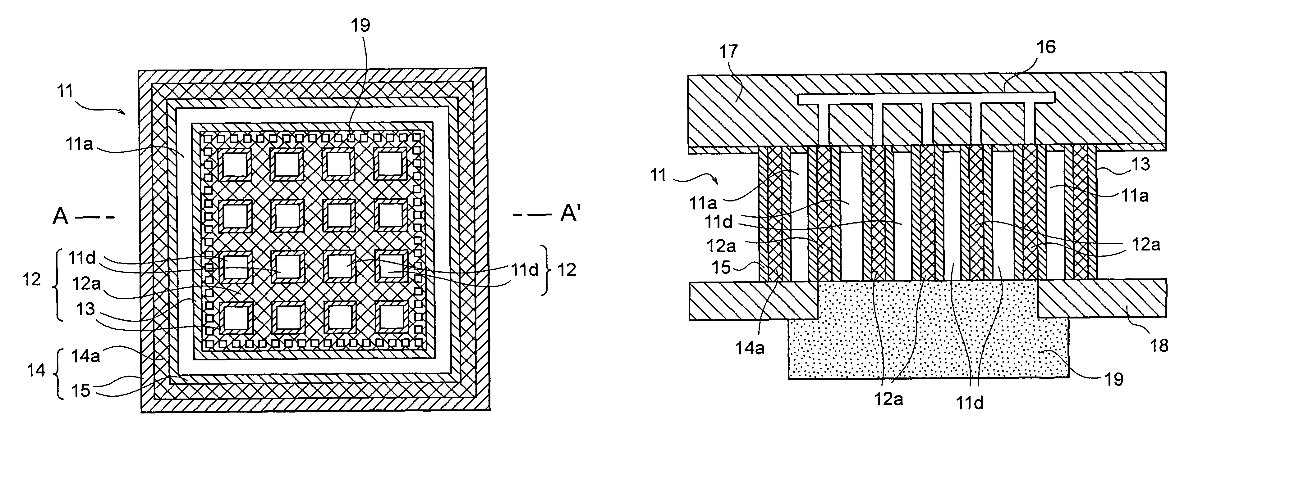
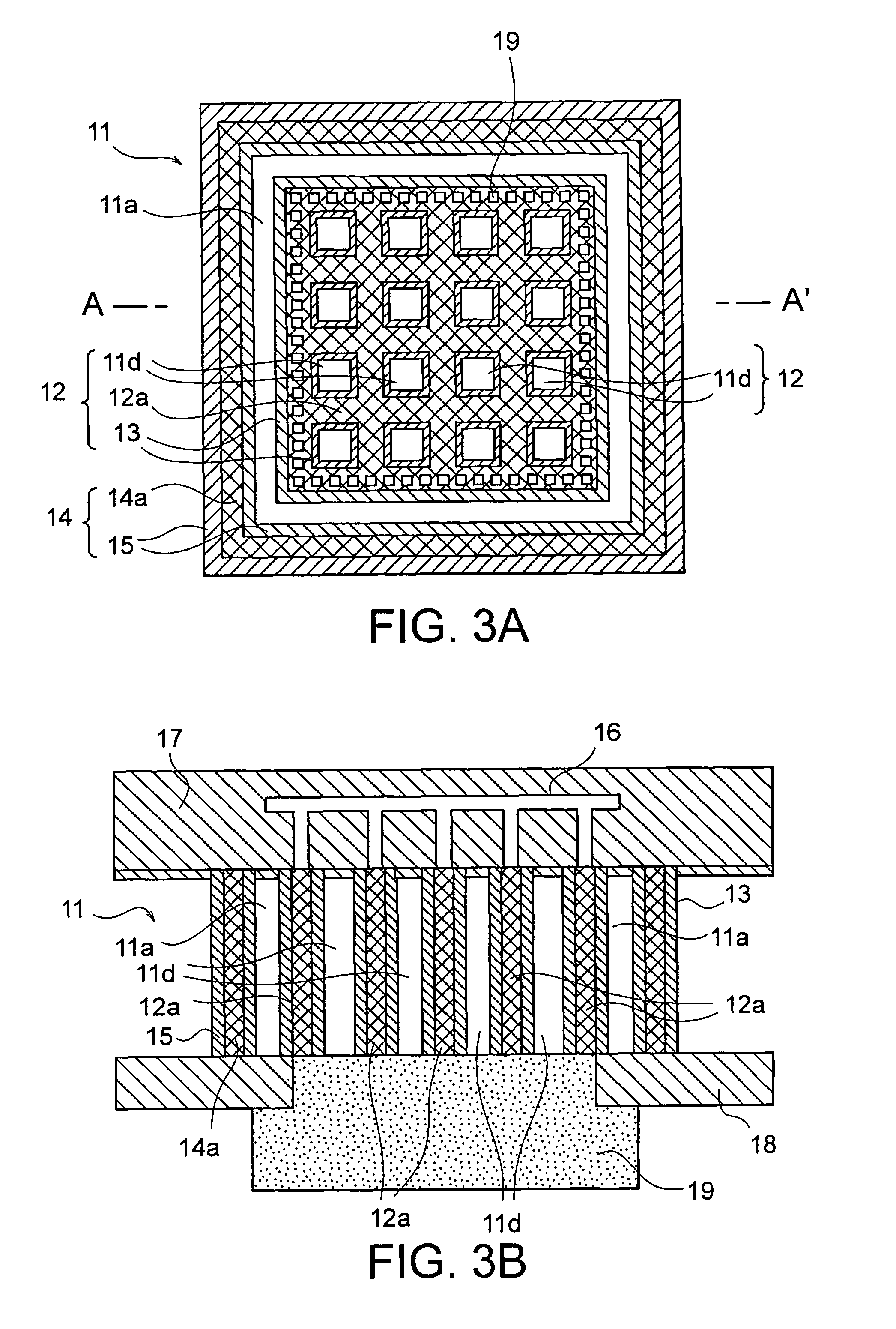
[0039]A preferred embodiment of the present invention will be described with reference to FIGS. 3A and 3B. FIGS. 3A and 3B show a structure of a through electrode according to the present invention. FIG. 3A is a plan view showing the structure of the through electrode, and FIG. 3B is a cross-sectional view taken along line A-A′ of FIG. 3A.

[0040]The through electrode of the present invention has a double through electrode structure including an inner through electrode 12 and a peripheral through electrode 14 in a semiconductor substrate 11. The peripheral through electrode 14 is formed like a ring in the semiconductor substrate 11. An annular semiconductor 11a is formed inside of the peripheral through electrode 14. The inner through electrode 12 is formed so as to be surrounded by the annular semiconductor 11a. The inner through electrode 12 serves as an actual through electrode. No potential is supplied to the peripheral through electrode 14 and the annular semiconductor 11a, which...


PUM


Abstract

A method of manufacturing a through electrode. While using at least a first conductive film for a gate electrode as a mask, an inner trench and a peripheral trench is formed. The Inner trench is provided for an inner through electrode having a columnar semiconductor. The peripheral trench is provided for a peripheral through electrode around an annular semiconductor surrounding the inner trench. The inner trench and the peripheral trench are filled with a through electrode insulation film and a through electrode conductive film, respectively, to form an inner through electrode and a peripheral through electrode.

Description

[0001]This application claims priority to prior Japanese patent application JP 2005-357819, the disclosure of which is incorporated herein by reference.BACKGROUND OF THE INVENTION[0002]The present invention relates to a semiconductor device, and more particularly to a semiconductor device having a through electrode which forms a three-dimensional semiconductor device, and to a method of manufacturing such a semiconductor device.[0003]Three-dimensional semiconductor devices having a plurality of stacked semiconductor devices have been proposed in recent years. In these three-dimensional semiconductor devices, the respective semiconductor devices are electrically connected to each other by through electrodes, which extend through semiconductor substrates.[0004]FIGS. 1 and 2 show a conventional three-dimensional semiconductor device. The three-dimensional semiconductor device shown in FIG. 1 has three semiconductor devices 3, 4, and 5 and a support substrate 1 on which the semiconducto...

Claims


Application Information

Patent Timeline
Patent Type & Authority Patents(United States)
IPC IPC(8): H01L23/48H01L21/4763
CPCH01L21/76898H01L23/481H01L25/0657H01L25/50H01L2224/16225H01L2225/06541H01L2225/06582H01L2224/16145H01L2225/06513H01L24/03H01L2224/05001H01L2224/05009H01L2224/051H01L2224/056H01L2224/06131H01L2224/13025H01L2924/00014
Inventor UCHIYAMA, SHIRO
Owner MICRON TECH INC
Why Eureka
Try Eureka