Developing device, memory unit thereof, and image forming apparatus

a technology of developing device and memory unit, which is applied in the direction of electrographic process apparatus, instruments, optics, etc., can solve the problems of memory unit damage, memory unit damage by heat, limited life span of developing device, etc., to prevent memory unit damage and poor connection, and improve the mounting position of memory unit

Active Publication Date: 2010-06-22
HEWLETT PACKARD DEV CO LP
View PDF19 Cites 22 Cited by
  • Summary
  • Abstract
  • Description
  • Claims
  • Application Information

AI Technical Summary

Benefits of technology

[0014]The present general inventive concept provides a developing device to prevent damage of a memory unit and poor connection between terminals of the memory unit and a main body of an image forming apparatus, by improving a mounting position of the memory unit, and an image forming apparatus having the same.

Problems solved by technology

Since a life span of the developing device is limited, the developing device has to be replaced when exhausted.
For example, if the memory unit is disposed around a fixing device which generates a lot of heat, the memory unit would be damaged by the heat.
If the fixing device is disposed around the photoconductive medium or developing rollers, the terminals of the memory unit would be easily contaminated by developers scattering about from the photoconductive medium or the developing rollers.
This will deteriorate the connection between the memory unit and the image forming apparatus.
Furthermore, if the memory unit is disposed at a position such as an upper or lower surface of the developing device often interfered with by other component parts in the image forming apparatus when the developing device is mounted, the memory unit terminals are apt to be damaged during mounting of the developing device.
Moreover, when the memory unit is disposed at a position subject to vibration generated from the developing device in operation, the electric connection between the memory unit and the image forming apparatus becomes unstable due to the vibration transmitted to the memory unit.

Method used


Image

  • Developing device, memory unit thereof, and image forming apparatus
  • Developing device, memory unit thereof, and image forming apparatus
  • Developing device, memory unit thereof, and image forming apparatus

Examples


Embodiment Construction

[0046]Reference will now be made in detail to exemplary embodiments of the present general inventive concept, examples of which are illustrated in the accompanying drawings, wherein like reference numerals refer to like elements throughout. The embodiments are described below to explain the present general inventive concept by referring to the figures.

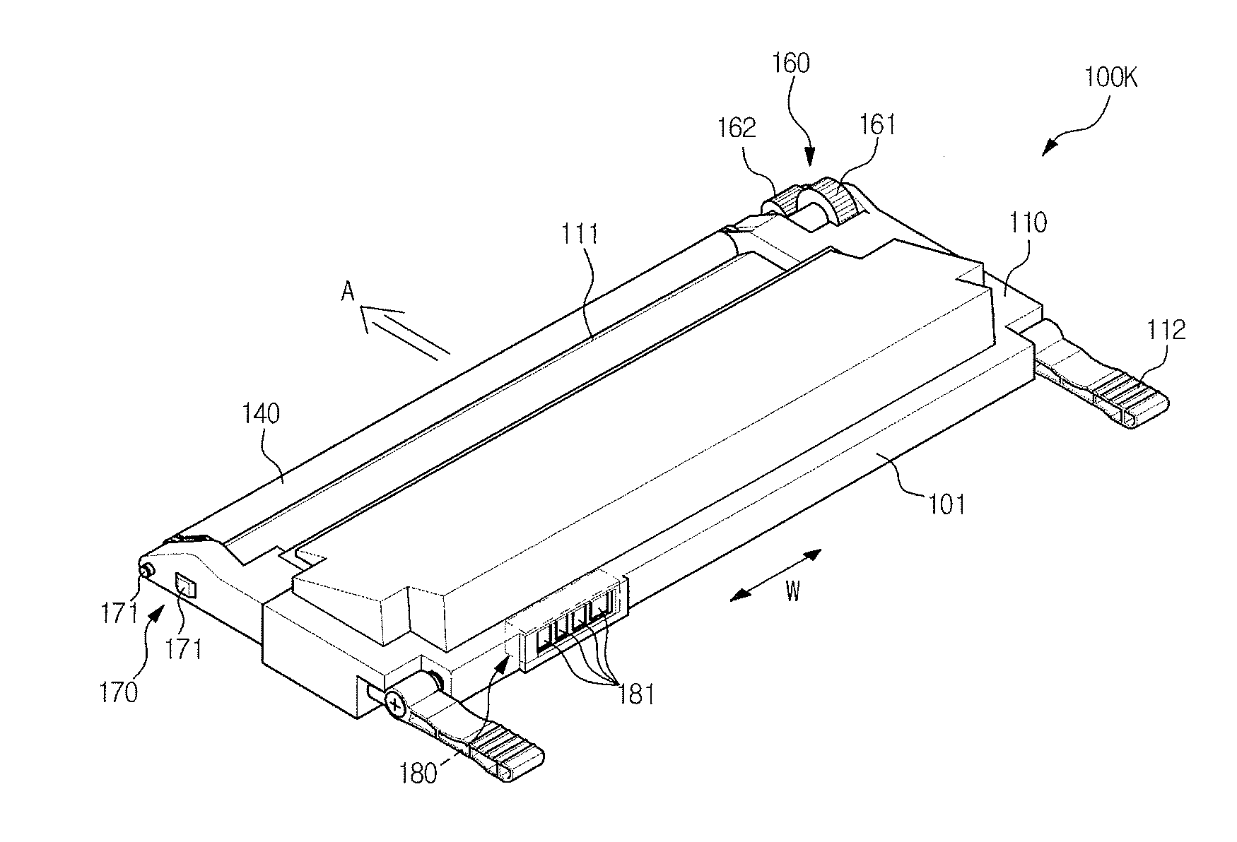
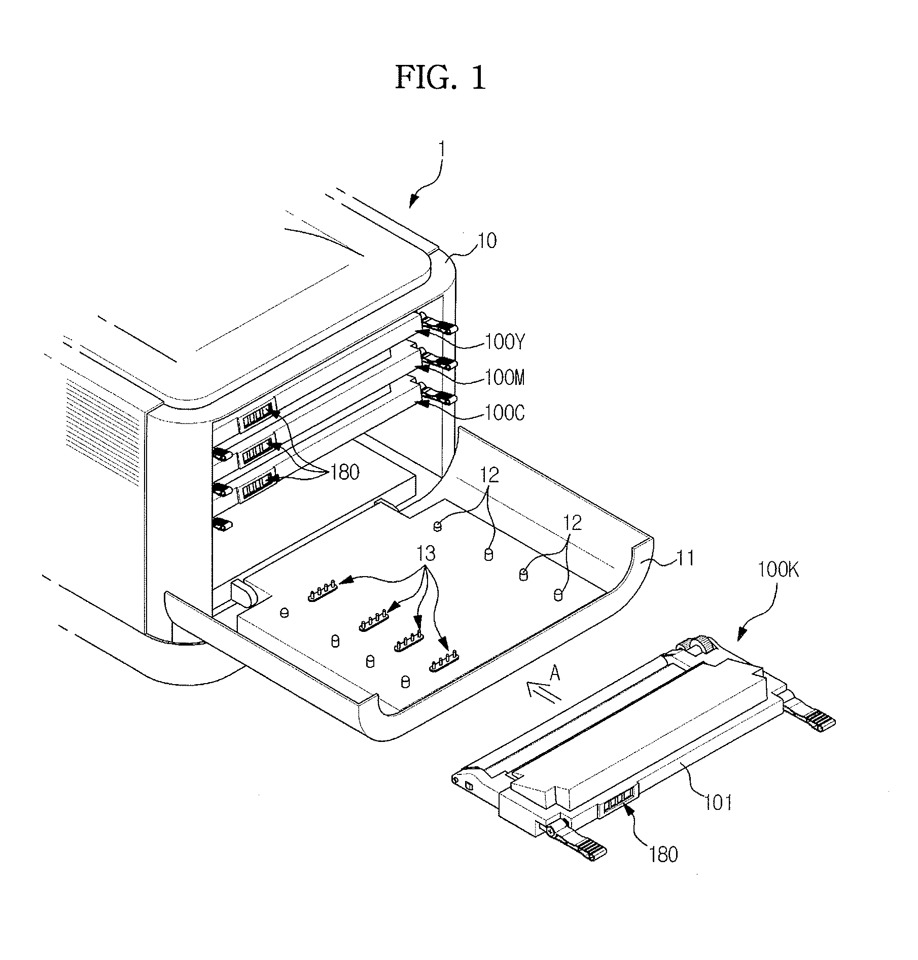
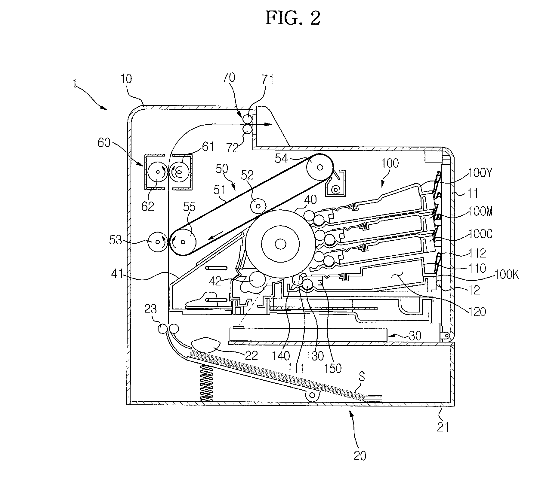
[0047]FIG. 1 is a perspective view illustrating an image forming apparatus according to an embodiment of the present general inventive concept, and FIG. 2 is a view illustrating a structure of the image forming apparatus illustrated in FIG. 1. Referring to the FIG. 1 and FIG. 2, the image forming apparatus 1 includes a main body 10, a printing medium feeding device 20, a laser scanning device 30, a photoconductive medium 40, a developing device 100, a transferring device 50, a fixing device 60, and a printing medium discharging device 70.

[0048]Especially, the present embodiment will be explained regarding a color image forming apparatu...


PUM


Abstract

A developing device to prevent damage of a memory unit and poor connection between terminals of the memory unit and a main body of an image forming apparatus, by improving a mounting position of the memory unit. The developing device is removably mounted to a main body of the image forming apparatus. The memory unit includes terminals exposed through a rear side of the developing device. The memory unit is disposed closer to a power reception unit formed at one side of the developing device than to a driving force reception unit formed at an other side of the developing device.

Description

CROSS-REFERENCE TO RELATED APPLICATIONS[0001]This application claims priority under 35 U.S.C. §119(a) from Korean Patent Application No. 2008-0018969 filed on Feb. 29, 2008 and No. 2007-0091999 filed on Sep. 11, 2007, in the Korean Intellectual Property Office, the disclosures of which are incorporated herein in their entirety by reference.BACKGROUND OF THE INVENTION[0002]1. Field of the Invention[0003]The present general inventive concept relates to an image forming apparatus, and more particularly to a developing device with a memory unit, and an image forming apparatus having the same.[0004]2. Description of the Related Art[0005]Generally, an image forming apparatus produces an image on a printing medium in accordance with an input image signal. For example, a printer, a photocopier, a facsimile, and a multifunction peripheral (MFP) having combined functions of the aforementioned apparatuses belong to the image forming apparatus.[0006]Especially, an electrophotographic image form...

Claims


Application Information

Patent Timeline
Patent Type & Authority Patents(United States)
IPC IPC(8): G03G15/00
CPCG03G15/0896G03G15/553G03G15/0863G03G15/556G03G2215/0174G03G2215/0697G03G2221/166G03G2221/1846G03G2221/1657
Inventor KIM
Owner HEWLETT PACKARD DEV CO LP
Why Eureka
Try Eureka