Nitride-based semiconductor device with reduced leakage current

a technology of nitride-based semiconductors and leakage current, which is applied in the direction of semiconductor devices, electrical equipment, transistors, etc., can solve the problems of power loss or performance characteristics deterioration, the substrate is difficult to dicing for its hardness, and the apphire substrate has a weakness, so as to achieve the effect of reducing current leakag

Inactive Publication Date: 2010-06-29
SANKEN ELECTRIC CO LTD
View PDF14 Cites 12 Cited by
  • Summary
  • Abstract
  • Description
  • Claims
  • Application Information

AI Technical Summary

Benefits of technology

[0009]It is therefore an object of this invention to minimize current leakage in semiconductor devices of the kind having a main semiconductor region formed on a silicon or silicon compound substrate via a nitride semiconductor buffer region.
[0010]Stated briefly in one aspect thereof, the present invention provides a nitride-based semiconductor device such for example as a HEMT, MESFET or FET. Included is a substrate of silicon or silicon compounds such as silicon carbide or polycrystalline silicon. A main semiconductor region, which may be variously composed and configured depending upon the particular semiconductor device to be made, is formed on the silicon-containing substrate via a buffer region of a nitride-based semiconductor or semiconductors. A set of electrodes are connected to the main semiconductor region to complete the desired semiconductor device. The invention is best characterized by the fact that at least either of the buffer region and the main semiconductor region is adapted to provide a pn junction or junctions, either in the buffer region or between the buffer region and the main semiconductor region, for preventing current leakage therethrough.
[0011]Another aspect of the invention is such that a p-type impurity is introduced into at least part of the buffer region which, before introduction of the p-type impurity, has been either of a doped n-type nitride-based semiconductor or an undoped, substantially n-type (i.e., n-like) nitride-based semiconductor. Upon introduction of the p-type impurity, that at least part of the buffer region may either gain a p-type conductivity or become electrically resistive enough to prevent current leakage.

Problems solved by technology

The sapphire substrate had, however, a weakness of being difficult of dicing for its hardness, in addition to being expensive.
However, when formed on a silicon or silicon compound substrate, which is low in electrical resistance, the multilayered buffer region has proved to possess its own drawbacks.
The current leakage is of course a cause for power loss or a deterioration of performance characteristics.
Further, in cases where the voltage-withstanding capability of the device is determined on the basis of the magnitude of leakage current, that capability was evaluated to be very low.
Such aluminum nitride layers would give rise both to a lattice mismatch with the neighboring gallium nitride layers and to a difference in coefficient of thermal expansion, such that the aluminum nitride layers might be subjected to tensile stresses.
The result would be the cracking of the multilayered buffer region or of the main semiconductor region formed thereon.

Method used


Image

  • Nitride-based semiconductor device with reduced leakage current
  • Nitride-based semiconductor device with reduced leakage current
  • Nitride-based semiconductor device with reduced leakage current

Examples


embodiment

of FIG. 5

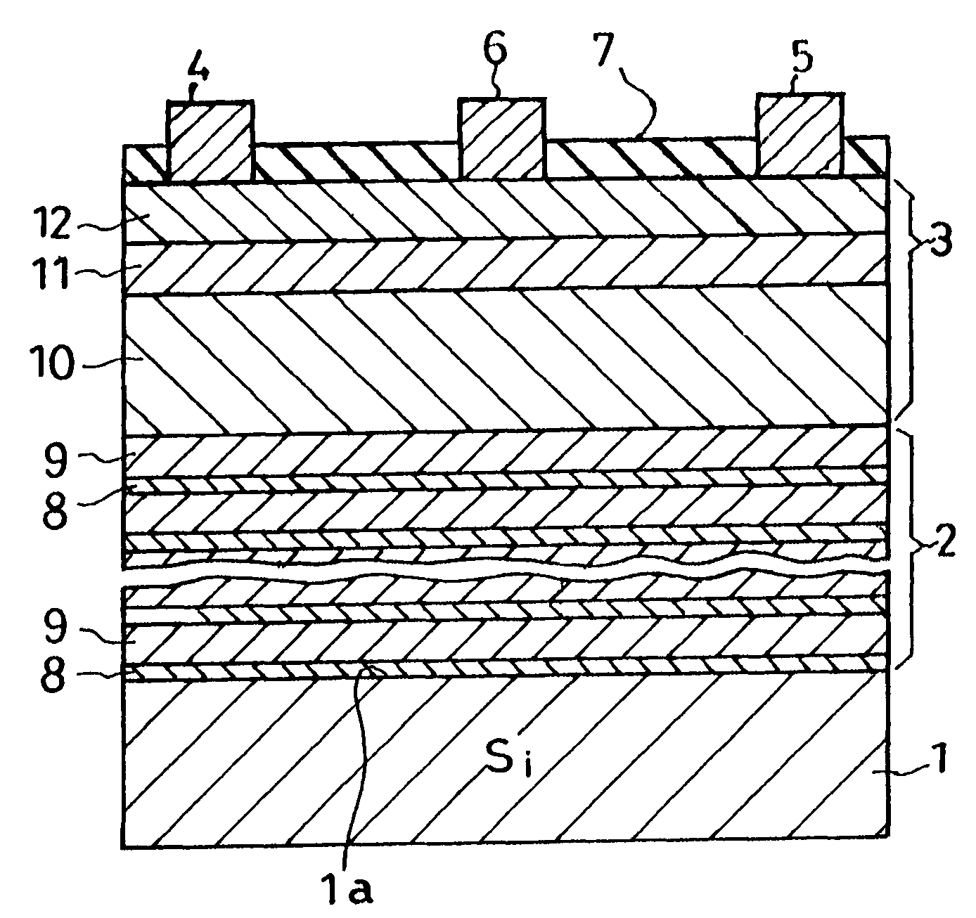
[0074]The multilayered buffer region 2 of the FIG. 1 embodiment is modifiable as indicated in FIG. 5. Generally designated 2a, the modified multilayered buffer region differs from its FIG. 1 counterpart 2 in that a p-type impurity (e.g. magnesium) is introduced into the first buffer layers 8a. The second buffer layers 9 are of p-type like that of FIG. 1, being doped with a p-type impurity. Thus the modified buffer region 2a comprises a required number of alternations of p-type first layers 8a and p-type second layers 9. The compositions of these buffer layers 8a and 9, aside from the p-type impurity, are the same as those of the buffer layers 8 and 9 of the FIG. 1 embodiment. The HEMT incorporating the modified buffer region 2a is identical with that of FIG. 1 in all the other details of construction.

[0075]Although the entire buffer region 2a is of p-type in this alternate embodiment, the pn junction remains between this p-type buffer region and the n-like electron transit ...


PUM

PropertyMeasurementUnit
thickaaaaaaaaaa
thickaaaaaaaaaa
thicknessaaaaaaaaaa

Abstract

A high electron mobility transistor is disclosed which has a triple-layered main semiconductor region formed on a silicon substrate via a multilayered buffer region. The multilayered buffer region is in the form of alternations of an aluminum nitride layer and a gallium nitride layer. Whilst the aluminum nitride layers are of n-like conductivity, the gallium nitride layers are doped into p-type conductivity, with the consequent creation of pn junctions between the two kinds of buffer layers. Another pn junction is formed between one p-type gallium nitride layer and the adjoining n-like electron transit layer included in the main semiconductor region. The pn junctions serve for reduction of current leakage.

Description

CROSS REFERNCE TO RELATED APPLICATIONS[0001]This is a continuation of Application PCT / JP2004 / 011058, filed Aug. 2, 2004, which claims priority to Japanese Patent Application No. 2003-289983 filed Aug. 8, 2003.BACKGROUND OF THE INVENTION[0002]This invention relates to semiconductor devices, particularly to those of the class employing nitrides or nitride-based compounds as semiconductors, as typified by metal semiconductor field-effect transistors (MESFETs) and high electron mobility transistors (HEMTs), and more particularly to such semiconductor devices of reduced leakage current. The invention also specifically pertains to a method of making such semiconductor devices.[0003]The gallium-nitride-based semiconductor devices were known and used extensively which had the gallium-nitride-based semiconductor region formed on a sapphire substrate via a buffer region. The sapphire substrate had, however, a weakness of being difficult of dicing for its hardness, in addition to being expensi...

Claims


Application Information

Patent Timeline
Patent Type & Authority Patents(United States)
IPC IPC(8): H01L29/20H01L29/778
CPCH01L29/7787H01L21/02381H01L21/02458H01L21/02507H01L21/0254H01L21/02579H01L21/0262H01L29/2003H01L21/02576H01L29/1075
Inventor OTSUKA, KOJICHINO, EMIKOYANAGIHARA, MASATAKA
Owner SANKEN ELECTRIC CO LTD
Why Eureka
Try Eureka