Substrate supports for semiconductor applications

Active Publication Date: 2012-06-07
FM INDS
View PDF2 Cites 53 Cited by
  • Summary
  • Abstract
  • Description
  • Claims
  • Application Information

AI Technical Summary

Benefits of technology

[0016]This invention provides coated substrate supports, e.g., coated electrostatic chucks, in which the coating can minimize current leakage from the electrostatic chuck, eliminate concern about the electrostatic attraction force varying depending on the type of workpiece mounted on the support surface, advantageously enhance the attractive or chucking force, and also facilitate de-chucking.
[0017]This invention also provides coated substrate supports, e.g., coated electrostatic chucks, that have improved eros

Problems solved by technology

Some minimal current passes between the chuck surface and the substrate at the contact point but generally not enough to result in device damage.
As the plasma provides a current path between the electrostatic chuck and the chamber sidewalls that are normally grounded, the movement of charge through the body is diverted from the support surface to ground, substantially reducing the charge accumulation on the support surface resulting in diminished or lost attractive force.
A dislodged substrate is likely to become damaged or improperly processed.
Problems associate

Method used


Image

  • Substrate supports for semiconductor applications
  • Substrate supports for semiconductor applications
  • Substrate supports for semiconductor applications

Examples


example 1

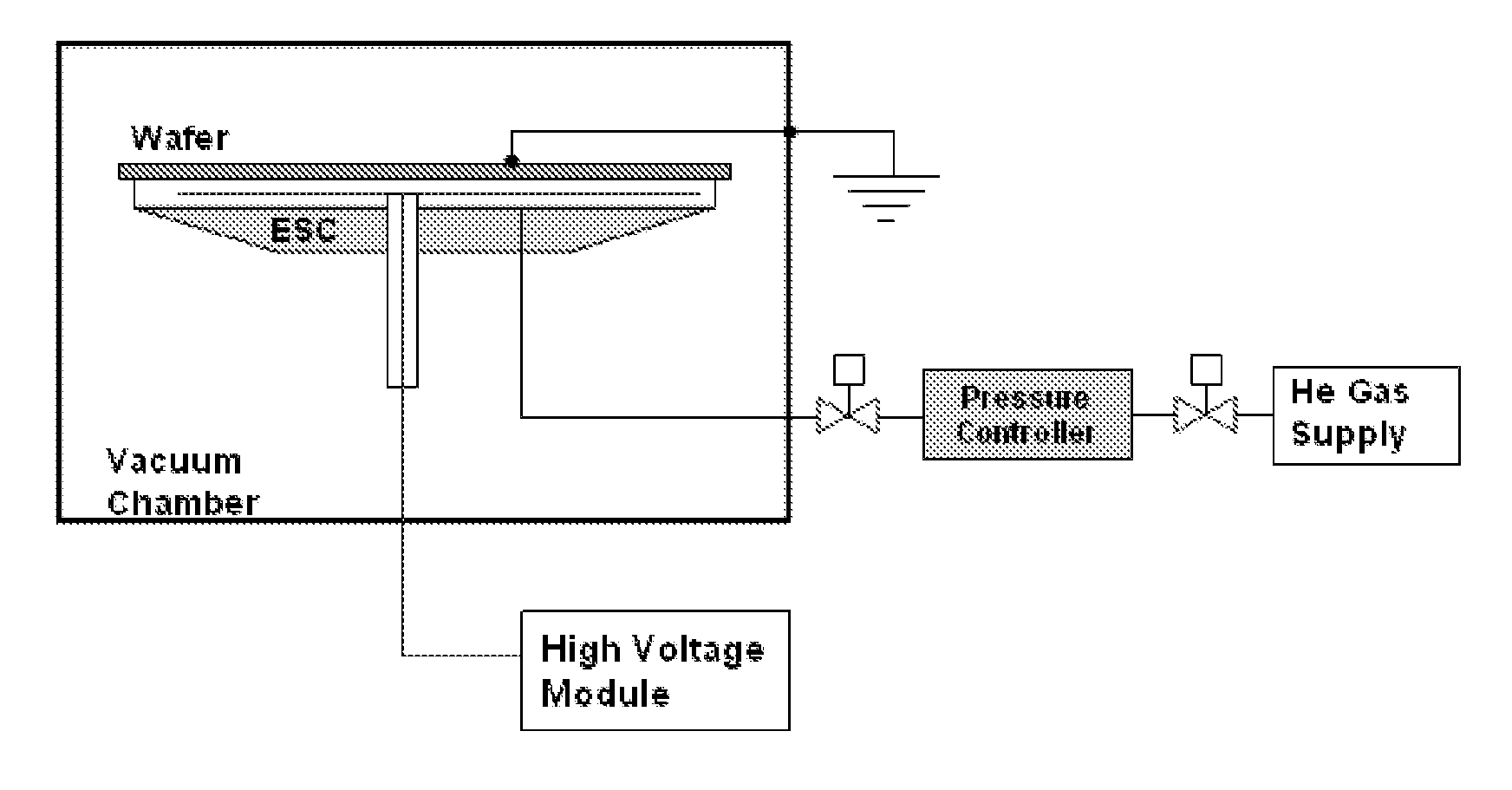
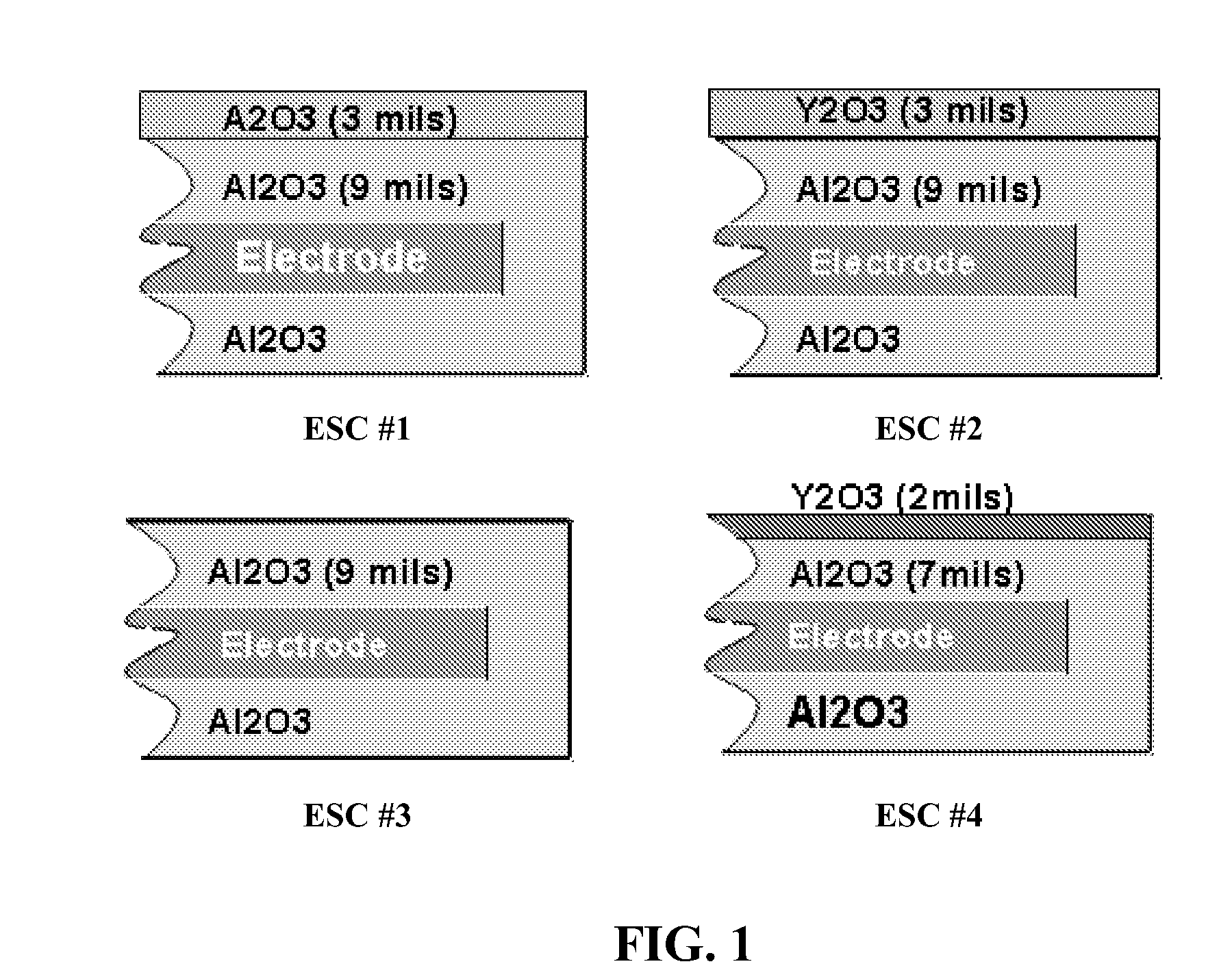
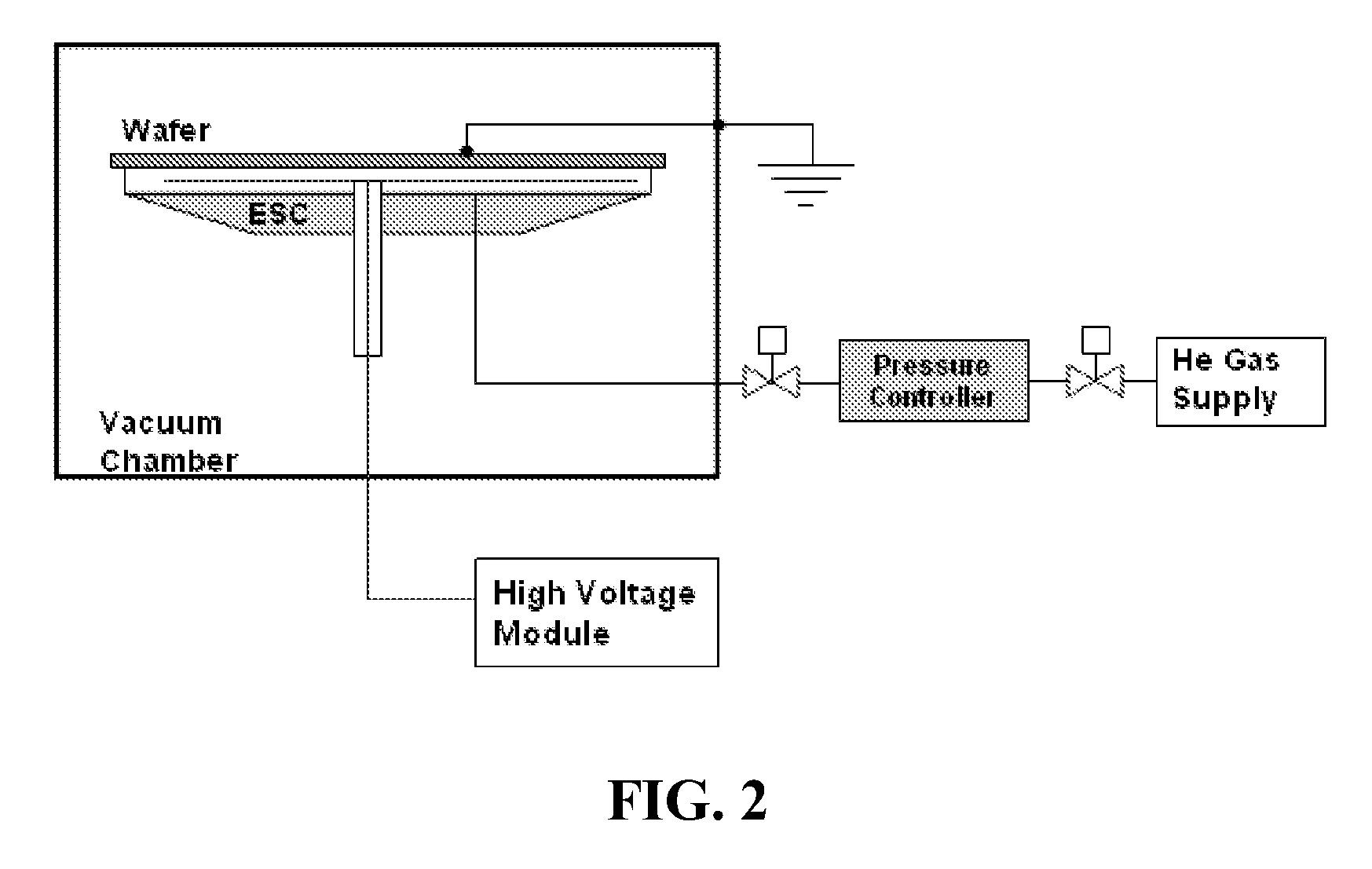
[0072]Four different electrostatic chucks (ESCs) for a 300 mm wafer were fabricated to compare chucking force. The four ESCs are shown in cross section in FIG. 1. ESC #1 and ESC#2 were one test set and ESC #3 and ESC#4 were another test set. ESC #1 was coated with an Al2O3 undercoat layer (9 mils) and an Al2O3 topcoat layer (3 mils). ESC #2 was coated with an Al2O3 undercoat layer (9 mils) and a Y2O3 topcoat layer (3 mils). ESC #3 was coated with a single Al2O3 layer (9 mils). ESC #4 was coated with an Al2O3 undercoat layer (7 mils) and a Y2O3 topcoat layer (2 mils).

[0073]In order to make sure that the factors affecting on chucking force such as surface roughness of the ESC surface contacting the wafer and contact ratio with the wafer, the resistance of each layer and thickness were checked before the chucking force was measured.

[0074]In order to measure the chucking force, gas was introduced in between the wafer and each ESC and the flow rate of the gas leaking through the peripher...

example 2

[0084]Plasma resistance was determined for the yttria topcoat layer. The measurement technique utilized to obtain this data was very precise, i.e., + / −0.5 micrometers. A Zeiss Confocal microscope (CSM 700) was used to measure the step height. Coating surfaces were polished to very smooth finishes (i.e., about 7 microns) in order to ensure the step height due to plasma erosion could clearly be differentiated. The number of measurements per sample and the number of replicates are provided in FIG. 4. The magnitudes measured were after 60 total hours of exposure. The data shows that yttria erodes about 2-3 micrometers after 60 hours of exposure with CF4 / O2 reactive ion etching (RIE). In comparison, the data shows that alumina erodes about 16 micrometers after 60 hours with CF4 / O2 RIE. This amounts to an erosion rate of about 5-8×greater for alumina as compared to yttria.

example 3

[0085]Al2O3 is typically used for parts exposed to plasma in a plasma process chamber. The reaction of Al2O3 with gases including fluorine (e.g., NF4 or CF4 to be used for cleaning in a deposition process and etchant in an etch process) produces AlF on the Al2O3 surface. This causes a particle issue resulting in changes in material properties and process drift with time. In accordance with this invention, a Y2O3 coating on top of Al2O3 can be used as the dielectric material for an ESC. A Y2O3 coating on top of Al2O3 is also desirable because Y2O3 does not react with fluorine.


PUM


Abstract

This invention relates to substrate supports, e.g., coated electrostatic chucks, having a dielectric multilayer formed thereon; dielectric multilayers that provide erosive and corrosive barrier protection in harsh environments such as plasma treating vessels used in semiconductor device manufacture; process chambers, e.g., deposition chambers, for processing substrates; methods for protecting substrate supports; and methods for producing substrate supports and electronic devices. The dielectric multilayer comprises (a) an undercoat dielectric layer comprising a metal oxide or metal nitride formed on a surface; and (b) a topcoat dielectric layer comprising a metal oxide formed on the undercoat dielectric layer. The topcoat dielectric layer has an aluminum oxide content of less than about 1 weight percent. The topcoat dielectric layer has a corrosion resistance and/or plasma erosion resistance greater than the corrosion resistance and/or plasma erosion resistance of the undercoat dielectric layer. The undercoat dielectric layer can have a resistivity greater than the resistivity of the topcoat dielectric layer. The topcoat dielectric layer can have a dielectric constant greater than the dielectric constant of the undercoat dielectric layer. The undercoat dielectric layer can have a porosity greater than the porosity of the topcoat dielectric layer. The invention is useful, for example, in the manufacture and protection of electrostatic chucks used in semiconductor device manufacture.

Description

RELATED APPLICATIONS[0001]The present application claims priority to U.S. Provisional Application Ser. No. 61 / 349,544, filed May 28, 2010, which is incorporated by reference herein in its entirety.FIELD OF THE INVENTION[0002]This invention relates to substrate supports, e.g., electrostatic chucks, having a dielectric multilayer formed thereon; dielectric multilayers that provide erosive and corrosive barrier protection in harsh environments such as plasma treating vessels used in semiconductor device manufacture; process chambers, e.g., deposition chambers, for processing substrates; methods for protecting substrate supports; and methods for producing substrate supports and electronic devices. The invention is useful, for example, in the manufacture and protection of electrostatic chucks used in semiconductor device manufacture.BACKGROUND OF THE INVENTION[0003]Electrostatic chucks are widely used to hold substrates, such as semiconductor wafers, in stationary position during substra...

Claims


Application Information

Patent Timeline
IPC IPC(8): H02N13/00B05D5/00B05D5/12
CPCH01L21/6833H01L21/6831
Inventor CHO, JAEYONGSIRMAN, JOHN
Owner FM INDS
Why Eureka
Try Eureka