High density antifuse based partitioned FPGA architecture

a high density, anti-fuse technology, applied in the direction of instruments, pulse techniques, computations using denominational number representations, etc., can solve the problems of prohibitively long programming time of the fpga, large total fuse leakage during the normal operation of a large anti-fuse-based fpga, and limited capacitive nets of routing conductors with antifuses on them

Inactive Publication Date: 2003-10-30
MICROSEMI SOC
View PDF3 Cites 0 Cited by
  • Summary
  • Abstract
  • Description
  • Claims
  • Application Information

AI Technical Summary

Benefits of technology

[0009] It is a further object of the present invention to reduce the programming time in a large antifuse based FPGA.
[0010] It is a further object of the present invention to reduce the standby current in a large antifuse based FPGA.
[0013] It is a further object of the present invention to provide a partitioned FPGA with fixed and segmented interconnect routing channels for minimal and predictable routing delay.
[0014] According to the present invention an antifuse based FPGA architecture is partitioned into repeatable blocks of logic modules to reduce the programming time of the array and to minimize parasitic capacitance and current leakage in the array. Further, by employing repeatable blocks, the size of the FPGA may be made larger with minimal changes to the architecture. Disposed along the edges of each repeatable blocks are interface buffers for connecting to adjacent blocks and to an interconnect matrix that is connectable blocks other than adjacent blocks. Disposed at regular intervals in the interconnect matrix are repeater buffers to limit the number of antifuses on a given track of the interconnect matrix, to minimize RC delay, and to avoid violating the Ipeak limit.
[0015] As a further aspect of the present invention, each of the repeatable blocks may have a separate Vpp. Once programming is completed, these separate Vpp's can be employed as separate Vcc's for each of the repeatable blocks so that the voltage level to a particular block can be lowered to minimize standby current when the inputs and outputs of that particular block are not switching.

Problems solved by technology

Since the peak current is a function of the programming current which decreases as processes shrink, long capacitive nets of routing conductors with antifuses on them are limited as to the amount of current which they can charge and discharge.
Further, the total fuse leakage during the normal operation of a large antifuse based FPGA can also be quite considerable.
Finally, for large antifuse based arrays, the programming time of the FPGA can also become prohibitively long, having a duration, for example, of up to four hours to program a 50K FPGA, and up to ten hours to program a 200K gate FPGA.

Method used


Image

  • High density antifuse based partitioned FPGA architecture
  • High density antifuse based partitioned FPGA architecture
  • High density antifuse based partitioned FPGA architecture

Examples


Embodiment Construction

[0022] Those of ordinary skill in the art will realize that the following description of the present invention is illustrative only and not in any way limiting. Other embodiments of the invention will readily suggest themselves to such skilled persons.

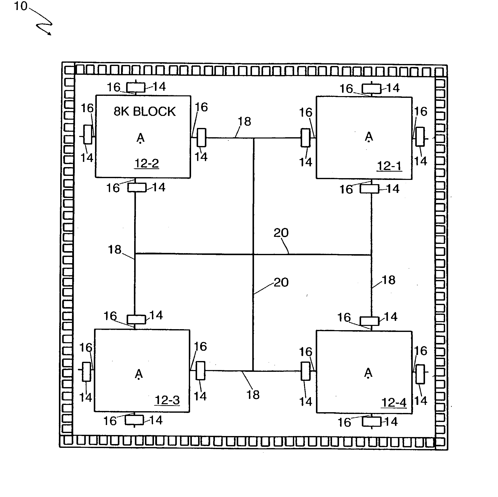
[0023] According to the present invention, FIG. 1 illustrates a partitioned FPGA architecture 10 including four blocks 12-1 through 12-4 of logic function modules laid out in a 2.times.2 grid pattern, bidirectional buffer banks 14, buffer channels 16, block interconnect channels 18 and routing channels 20. Also accompanying the partitioned FPGA architecture are I / O modules that are not shown to avoid overcomplicating the disclosure and thereby obscuring the present invention. It is presently contemplated that the I / O modules will be preferably disposed along the periphery of the FPGA architecture 10, and will be decoupled from the array. According to design choice the I / O modules can be modified based on the I / O requirements for differ...


PUM


Abstract

An antifuse based FPGA architecture is partitioned into repeatable blocks of logic modules to reduce the programming time of the array and to minimize parasitic capacitance and current leakage in the array. With repeatable blocks the size of the FPGA may be made larger with minimal changes to the architecture. Disposed along the edges of each repeatable block are bidirectional buffer banks for connecting to adjacent blocks and to an interconnect matrix that is connectable to blocks other than adjacent blocks. Disposed at regular intervals in the interconnect matrix are repeater buffers to limit the number of antifuses on a given track of the interconnect matrix, to minimize RC delay, and to avoid violating the Ipeak limit.

Description

[0001] 1. Field Of The Invention[0002] The present invention relates to an antifuse-based field programmable gate array (FPGA). More particularly, the present invention relates to a partitioned architecture for a high density antifuse based FPGA.[0003] 2. The Prior Art[0004] As is well understood by those of ordinary skill in the art, the architecture for an antifuse based FPGA typically includes logic modules which may be configured as logic gates that are connected together to form higher logic functions. The logic modules are connected together by routing conductors, and the connections are made by programming antifuses. As the number of gates included in an antifuse based FPGA increases, there are a number of considerations which place constraints on the size of the FPGA.[0005] As a first consideration, there is a limit on the number of antifuses that are ;lo permitted on any given routing conductor due to the amount of leakage current through and the resistive load across unpro...

Claims


Application Information

Patent Timeline
Patent Type & Authority Applications(United States)
IPC IPC(8): H03K19/177
CPCH03K19/17736H03K19/17796H03K19/1778
Inventor ASAYEH, REZA
Owner MICROSEMI SOC
Why Eureka
Try Eureka