Erase and program method of flash memory device for increasing program speed of flash memory device

a flash memory device and program method technology, applied in static storage, digital storage, instruments, etc., can solve the problems of high probability of fail in erase process of mlcs, increase overall program time, so as to reduce the overall program time, reduce the failure occurrence ratio, and improve the threshold voltage distribution of mlcs

Active Publication Date: 2009-05-26
SK HYNIX INC
View PDF13 Cites 22 Cited by
  • Summary
  • Abstract
  • Description
  • Claims
  • Application Information

AI Technical Summary

Benefits of technology

[0021]An advantage of the present invention is that it provides an erase method of a flash memory device, in which it can reduce the fail occurrence ratio when erasing MLCs, improve the threshold voltage distribution of MLCs and reduce an overall program time in a subsequent program operation by performing pre-programming so that a voltage range in which threshold voltages of MLCs are distributed can be reduced.
[0022]Another advantage of the present invention is that it provides a program method of a flash memory device, in which only MLCs or SLCs having a slow program speed are selected and programmed wherein the ISPP method is performed for program, so that an overall program time can be reduced.
[0023]Further another advantage of the present invention is that it provides a program method of a flash memory device, in which step voltages (i.e., an increment width of a program voltage) before and after threshold voltages of MLCs become a set verify voltage are set to be different from each other in the ISPP method for program, so that an overall program time can be reduced.
[0024]According to an aspect of the present invention, there is provided an erase method of a flash memory device including a plurality of MLCs that share word lines and bit lines, including the steps of pre-programming some of the plurality of MLCs so that a range in which threshold voltages of the plurality of MLCs are distributed is reduced, erasing the plurality of MLCs, and verifying whether the plurality of MLCs has been normally erased.
[0025]According to another aspect of the present invention, there is provided a program method of a flash memory device including a plurality of memory cells that share word lines and bit lines, including the steps of selecting one of the word lines; programming memory cells connected to the selected word line, of the plurality of memory cells, by applying a start program voltage to the selected word line; selecting memory cells respectively having threshold voltages lower than a predetermined voltage, of the memory cells connected to the selected word line; programming the selected memory cells by applying a pre-program voltage to the selected word line; prohibiting program into the remaining memory cells other than the selected memory cells when the selected memory cells are programmed; and additionally programming the memory cells connected to the selected word line, while supplying a program voltage that gradually rises from the start program voltage at the ratio of the step voltage to the selected word line.
[0026]According to further another aspect of the present invention, there is provided a program method of a flash memory device including a plurality of memory cells that share word lines and bit lines, including the steps of selecting one of the word lines; programming memory cells connected to the selected word line by applying a start program voltage that gradually rises at the ratio of a step voltage to the selected word line in each of first to Pth (P is an integer) program cycles; selecting memory cells respectively having threshold voltages lower than a predetermined voltage, of the memory cells connected to the selected word line; programming the selected memory cells by applying a pre-program voltage to the selected word line; prohibiting program into the remaining memory cells other than the selected memory cells when the selected memory cells are programmed; and additionally programming the memory cells connected to the selected word line, while supplying a program voltage that gradually rises from the start program voltage that has finally rises in the step of programming the memory cells at the ratio of the step voltage to the selected word line.

Problems solved by technology

Therefore, the probability that fail occurs in the erase process of the MLCs is high.
Furthermore, in the erase process of the flash memory device in the related art, MLCs have threshold voltages that are relatively widely distributed (i.e., not having a good threshold voltage distribution).
Therefore, a problem arises because an overall program time is increased in a subsequent program process.
If the number of the program cycles increased as described above, a problem arises because an overall program time is increased.
This problem also occurs even in a flash memory device having SLCs.

Method used


Image

  • Erase and program method of flash memory device for increasing program speed of flash memory device
  • Erase and program method of flash memory device for increasing program speed of flash memory device
  • Erase and program method of flash memory device for increasing program speed of flash memory device

Examples


first embodiment

[0164]FIG. 17 is a flowchart illustrating a program method according to the present invention. The program method is related to program of MLCs.

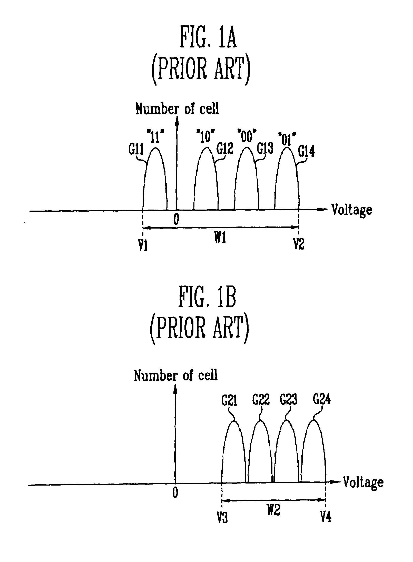
[0165]One (e.g., WL1) of the word lines WL1 to WLJ is selected (601). As a start program voltage (refer to VPA in FIG. 23) is applied to the selected word line WL1, the MLCs Me11 to Me1K or Mo11 to Mo1K connected to the selected word line WL1 are programmed (602). Thereafter, MLCs (e.g., Me11 to Me15 or Mo11 to Mo15), each having threshold voltages lower than a predetermined voltage, of the MLCs Me11 to Me1K or Mo11 to Mo1K, is selected (603). The step (603) will be described in more detail below with reference to FIG. 18.

[0166]The lower bit register 230 of each of the page buffers PB1 to PBK senses a voltage (e.g., VCC) of the sensing node SO in response to the read control signal (LREAD1) and stores the lower sensing data (SL1) of logic “0” depending on the sensing result, so that it is initialized.

[0167]Thereafter, as a verify voltage (re...

second embodiment

[0217]FIG. 24 is a flowchart illustrating a program method according to the present invention. This method is related to program of MLCs.

[0218]One (e.g., WL1) of the word lines WL1 to WLJ is selected (701). As a start program voltage (refer to VA1 in FIG. 25) is applied to the selected word line WL1, the MLCs Me11 to Me1K or Mo11 to Mo1K connected to the word line WL1 are programmed (702).

[0219]The operation of the page buffers PB1 to PBK in the step (702) is the same as that of the page buffers PB1 to PBK in the step (620), which have been described with reference to FIG. 20. Description thereof will be omitted.

[0220]Thereafter, it is determined whether the number of program cycles, which is being executed, is P (703). If the number of program cycles, which is being executed, is not P in the step (703), the start program voltage (VA1) is increased as much as the step voltage (VS) (704). As a result, the word line WL1 is supplied with a start program voltage (VA2) that has risen fro...

third embodiment

[0227]FIG. 27 is a flowchart illustrating a program method according to the present invention. This method is related to program of SLCs.

[0228]One (e.g., WL1) of the word lines WL1 to WLJ is selected (601′).

[0229]As the selected word line WL1 is supplied with a start program voltage (refer to VSA in FIG. 28), SLCs Me11 to Me1K or Mo11 to Mo1K connected to the selected word line WL1 are programmed (602′).

[0230]Thereafter, SLCs (e.g., Me11 to Me15 or Mo11 to Mo15), each having threshold voltages lower than a predetermined voltage, of the SLCs Me11 to Me1K or Mo11 to Mo1K, are selected (603′). Though detailed steps of the step (603′) has not been shown, the step (603′) can be performed in the same manner as that described with reference to FIG. 18.

[0231]The lower bit register 230 of each of the page buffers PB 1 to PBK senses a voltage (e.g., VCC) of the sensing node SO in response to the read control signal (LREAD1) and stores the lower sensing data (SL1) of logic “0” depending on the...


PUM


Abstract

Erase and program methods of a flash memory device including MLCs for increasing the program speed are described. In the erase method, MLCs are pre-programmed so that a voltage range in which threshold voltages of MLCs are distributed can be reduced. Therefore, a fail occurrence ratio can be reduced when erasing MLCs, the threshold voltage distribution of MLCs can be improved and an overall program time can be shortened in a subsequent program operation.

Description

FIELD OF THE INVENTION[0001]The present invention relates to flash memory devices, and more particularly, to erase and program methods of flash memory devices.DISCUSSION OF RELATED ART[0002]In general, memory cells of a flash memory device can be classified into a Single-Level Cell (hereinafter referred to as “SLC”) and a Multi-Level Cell (hereinafter referred to as “MLC”) depending on the number of data bits stored. One (1) bit data having a logic value of “1” or “0” can be stored in the SLC. Two (2) bits data having a logic value of any one of “11”, “10”, “01” and “00” can be stored in the MLC. Therefore, flash memory devices including MLCs are mainly used for high-integrated semiconductor devices requiring a large capacity of data space.[0003]An erase operation of the flash memory device including MLCs is performed is generally performed on a memory-cell-block basis. The erase operation includes a pre-program process, the erase process and a post program, which are sequentially e...

Claims


Application Information

Patent Timeline
Patent Type & Authority Patents(United States)
IPC IPC(8): G11C16/12G11C16/04G11C16/06G11C16/34
CPCG11C11/5628G11C11/5635G11C16/0483G11C16/12G11C16/16G11C16/3445G11C16/3459G11C2211/5621G11C2211/5642G11C16/14G11C16/26
Inventor HWANG, KYUNG PILKIM, HYUNG SEOKNOH, KEUM HWANKIM, JU INLEE, MIN KYUJOO, SEOK JINKIM, SOOK KYUNG
Owner SK HYNIX INC
Why Eureka
Try Eureka