Phase-change random access memory (PRAM) performing program loop operation and method of programming the same

a random access memory and program loop technology, applied in the field of semiconductor memory devices, can solve the problems of consuming a large amount of power using the programming loop approach, lengthening the overall programming time, etc., and achieves the effects of reducing current consumption, reducing overall programming time, and fast programming speed

Active Publication Date: 2009-08-11
SAMSUNG ELECTRONICS CO LTD
View PDF12 Cites 20 Cited by
  • Summary
  • Abstract
  • Description
  • Claims
  • Application Information

AI Technical Summary

Benefits of technology

[0021]Embodiments of the invention provide a PRAM performing a program loop operation having a reduced overall programming time and reduced current consumption. Embodiments of the invention also provide a method for programming such a PRAM. In at least one aspect, a PRAM designed and implemented according to an embodiment of the invention may omit unnecessary program loops in order to provide faster programming speeds with reduced current consumption.

Problems solved by technology

On the other hand, the iterative program loop approach lengthens the overall programming time.
Finally, a relatively large amount of power may be consumed using the programming loop approach.

Method used


Image

  • Phase-change random access memory (PRAM) performing program loop operation and method of programming the same
  • Phase-change random access memory (PRAM) performing program loop operation and method of programming the same
  • Phase-change random access memory (PRAM) performing program loop operation and method of programming the same

Examples


Embodiment Construction

[0032]Embodiments of the invention will be now described with reference to the accompanying drawings. The present invention may, however, be embodied in different forms and should not be constructed as being limited to only the illustrated embodiments. Rather, the embodiments are presented as teaching examples.

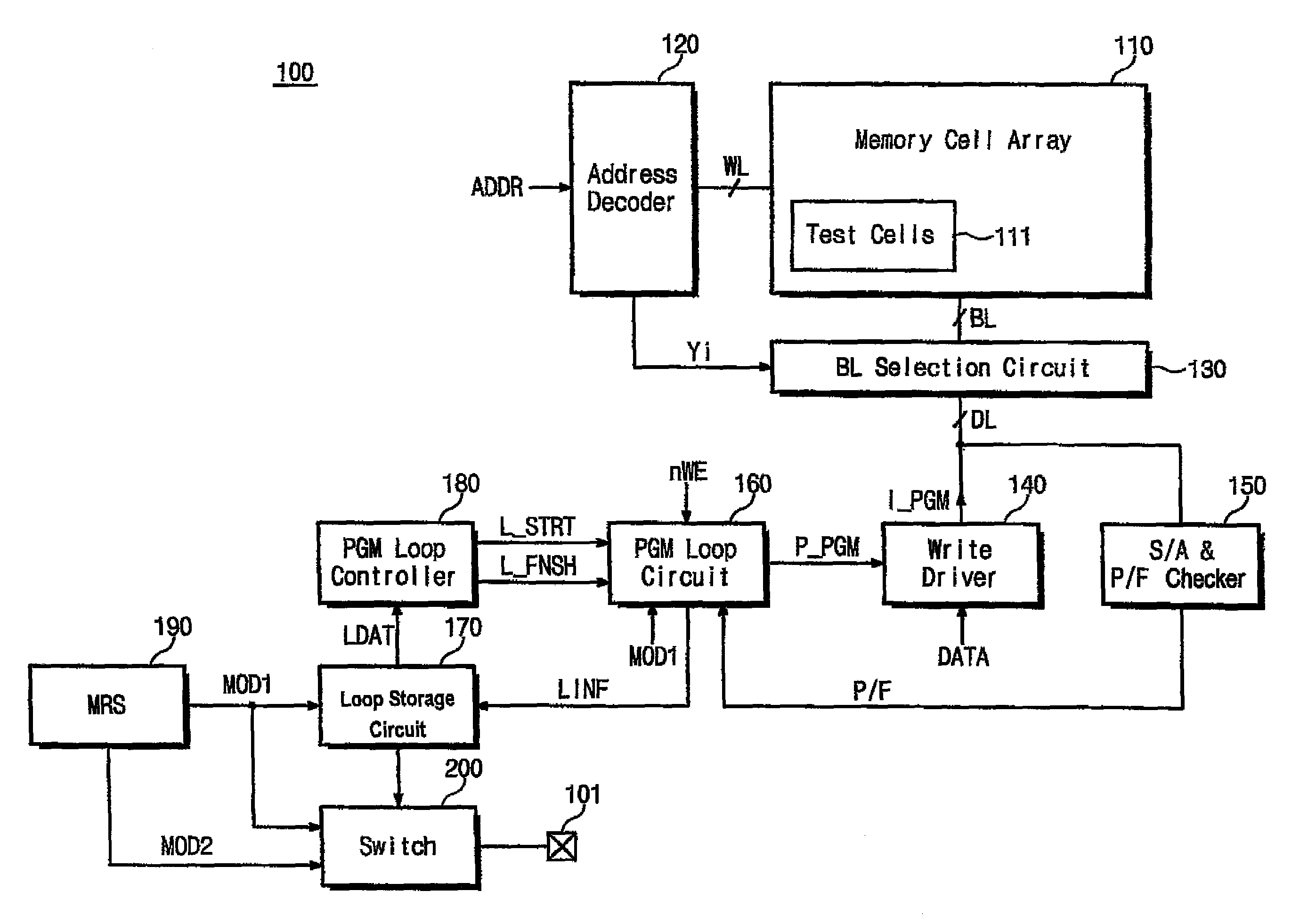
[0033]FIG. 4 is a block diagram illustrating a PRAM according to an embodiment of the invention. Referring to FIG. 4, a PRAM 100 includes a memory cell array 110, an address decoder 120, a BL selection circuit 130, a write driver 140, a sense amplification and verification circuit 150, and a program loop control unit. In the illustrated example, the program loop control unit includes a program loop circuit 160, a loop storage circuit 170, and a program loop controller 180.

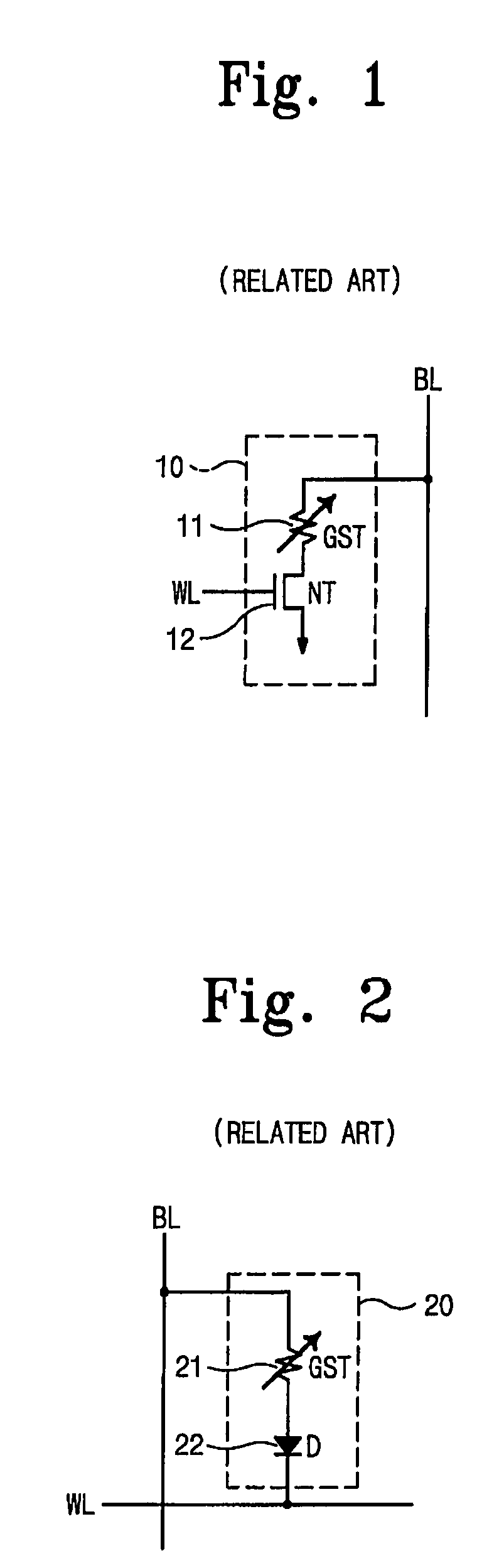
[0034]Memory cell array 110 includes a plurality of memory cells (not shown). Each memory cell includes a memory element and a select element. The memory element includes a phase change material and the corre...


PUM


Abstract

A PRAM and programming method are disclosed. The PRAM includes a memory cell array including a test cell, a write driver applying a program pulse and providing a program current to the memory cell array, a sense amplification and verification circuit reading data programmed in the memory cell array and performing a program verify operation on the data, and a program loop control unit storing program verification result for the test cell at each program loop during test operation and generating the program pulse according to the program verification result to control the start of the program loop during normal operation.

Description

CROSS-REFERENCE TO RELATED APPLICATIONS[0001]This U.S. non-provisional patent application claims priority under 35 U.S.C. § 119 to Korean Patent Application No. 10-2006-0089681, filed on Sep. 15, 2006, the subject matter of which is hereby incorporated by reference.BACKGROUND OF THE INVENTION[0002]1. Field of the Invention[0003]The present invention relates to a semiconductor memory device. More particularly, the invention relates to a PRAM performing program loop operations and a method of programming same.[0004]2. Description of the Related Art[0005]Semiconductor memory devices may be classified random access memory (RAM) devices and read only memory (ROM) devices. ROM is typically implemented as a nonvolatile memory that retains stored data when power is not applied. Examples of ROM are Programmable ROM (PROM), Erasable PROM (EPROM), Electrically EPROM (EEPROM), Flash Memory, etc. Flash memory may be further classified as NOR flash memory and a NAND flash memory.[0006]RAM has con...

Claims


Application Information

Patent Timeline
Patent Type & Authority Patents(United States)
IPC IPC(8): G11C7/22
CPCG11C13/0004G11C13/0064G11C13/0069G11C29/02G11C29/028G11C29/24G11C29/50G11C29/021G11C2213/79G11C13/004G11C16/3436G11C29/787G11C2213/72
Inventor PARK, JOON-MINKIM, DU-EUNG
Owner SAMSUNG ELECTRONICS CO LTD
Why Eureka
Try Eureka