Semiconductor device, semiconductor device testing method, and programming method

a technology of semiconductor devices and programming methods, applied in the direction of static storage, digital storage, instruments, etc., can solve the problems of not specifically revealing how the optimum programming conditions such as program widths are actually determined, and the document does not specifically disclose how. , to achieve the effect of reducing the number of pulses, and reducing the number of programming times

Inactive Publication Date: 2006-04-13
VALLEY DEVICE MANAGEMENT
View PDF14 Cites 21 Cited by
  • Summary
  • Abstract
  • Description
  • Claims
  • Application Information

AI Technical Summary

Benefits of technology

[0047] In accordance with the present invention, when programming is to be performed at multiple levels of a multilevel memory cell other than the last level, a programming operation is performed while the program voltage is increased stepwise. By doing so, overprogramming is prevented at the level other than the last level, and programming is performed using a program voltage with a greater pulse width at the last level. Thus, the programming time can be greatly shortened. By employing such a two-stage programming method, simultaneous programming in several memory cells can be performed. As a result, the programming time can be shortened.
[0048] The present invention also provides a programming method that includes the steps of: performing programming involved in multiple levels except a last level while increasing a program voltage stepwise; and performing programming involved in the last level while increasing the program voltage stepwise without verification for the programming until the program voltage reaches a given voltage. In accordance with the present invention, when programming is to be performed at the last level among several levels, a programming operation is performed while the program voltage is increased stepwise without verification until the program voltage reaches the predetermined voltage value. Thus, the time required for the programming operation at the last level can be greatly reduced.

Problems solved by technology

However, the document does not specifically disclose how the optimum programming conditions such as program widths are actually determined.
However, the document does not specifically disclose how the optimum voltage increase width is determined.

Method used


Image

  • Semiconductor device, semiconductor device testing method, and programming method
  • Semiconductor device, semiconductor device testing method, and programming method
  • Semiconductor device, semiconductor device testing method, and programming method

Examples


first embodiment

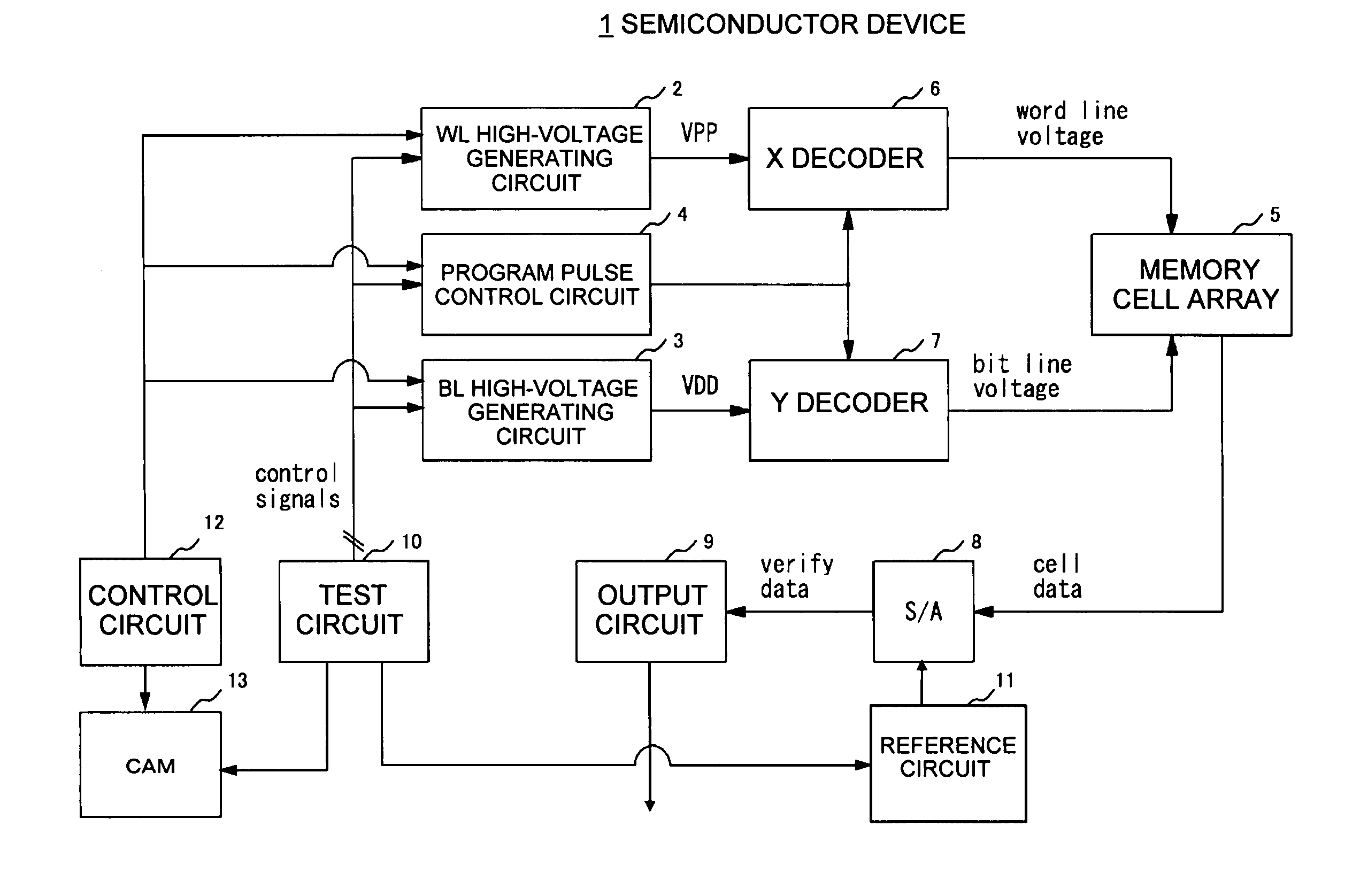
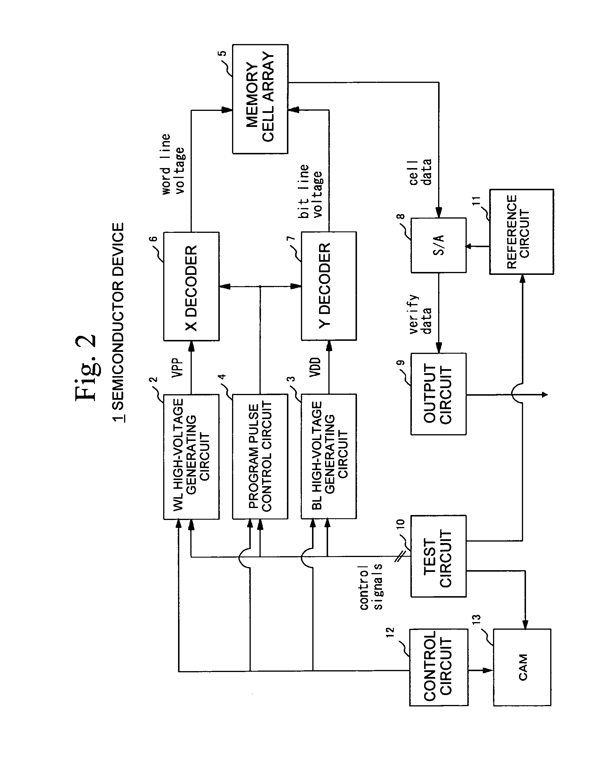
[0074] A first embodiment is now described. FIG. 2 is a block diagram of a semiconductor device 1 in accordance with the first embodiment. As shown in FIG. 2, the semiconductor device 1 includes a WL high-voltage generating circuit 2, a BL high-voltage generating circuit 3, a program pulse controller 4, a memory cell array 5, an X decoder, a Y decoder 7, a sense amplifier circuit 8, an output circuit 9, a test circuit 10, a reference circuit 11, a control circuit 12, and a CAM 13. The semiconductor device 1 may be a semiconductor memory device such as a flash memory that is packaged independently, or may be incorporated into a semiconductor device such as a system LSI.

[0075] The WL high-voltage generating circuit 2 in a test mode receives a control signal from the test circuit 10, and generates and supplies a booster voltage VPP to the X decoder 6. The X decoder 6 applies a word line voltage. The BL high-voltage generating circuit 3 in the test mode receives a control signal from t...

second embodiment

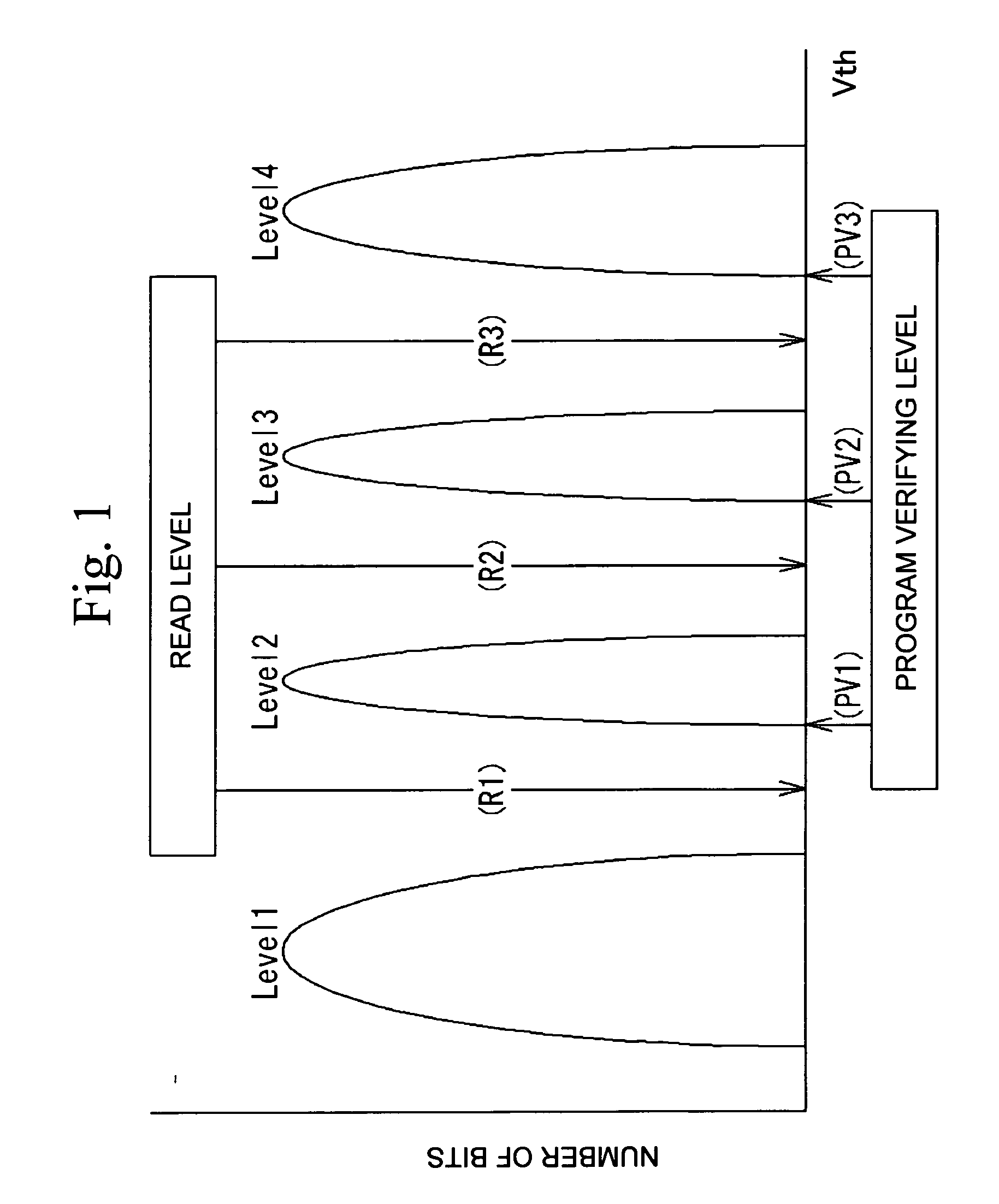
[0101] Next, a second embodiment of the present invention is described. The multi-value memories have four Vt levels of level 1, level 2, level 3, and level 4. Those four levels constitute two sets of output (or input) data. Here, level 1, level 2, level 3, and level 4 are defined as (1, 1), (0, 1), (1, 0), and (0, 0) as two sets of input / output data. When the data of level 4 is programmed, a programming technique by which a memory cell is programmed through each programming to level 2, level 3, and level 4 performed in order is generally used. By this technique, in the cells to be written at level 4, first, the cells are written to level 2 by a first programming flow.

[0102] Next, the cells are written to level 3 from level 2 by a second programming flow. Lastly, the cells are written to level 4 from level 3 by a third programming flow, and all the programming operations are ended. For the memory cells in which programming is required only up to level 2 or level 3, actual programmi...


PUM


Abstract

A semiconductor device includes: a latch circuit that latches a given signal in a test mode; and a generating circuit that generates a signal that defines a program voltage used for programming of a memory cell in accordance with the signal latched in the latch circuit. The generating circuit includes: a circuit that generates the signal that defines an initial voltage of the program voltage; a circuit that generates the signal that defines a pulse width of the program voltage; and a circuit that generates the signal that defines a step width of the program voltage when the program voltage is a voltage that increases stepwise.

Description

CROSS REFERENCE TO RELATED APPLICATIONS [0001] This is a continuation of International Application No. PCT / JP2004 / 012475, filed Aug. 30, 2004.BACKGROUND OF THE INVENTION [0002] 1. Field of the Invention [0003] The present invention relates to a semiconductor device, a testing method, and a programming method. [0004] 2. Description of the Related Art [0005] Semiconductor memories are generally classified into volatile memories from which information is erased when the power source is switched off, and non-volatile memories in which information is maintained even when the power source is switched off. As a representative type among the non-volatile memories, flash memories having the rewrite time shortened by collectively erase data are known. Examples of flash memories that are not affected by variations in device characteristics are described in the following. [0006] The device that is disclosed in Japanese Unexamined Patent Publication No. 2002-197880 determines the optimum program...

Claims


Application Information

Patent Timeline
Patent Type & Authority Applications(United States)
IPC IPC(8): G11C7/00
CPCG11C16/04G11C16/12G11C29/02G11C29/021G11C29/028G11C29/50G11C29/50004G11C2029/5004G11C16/06G11C16/10G11C29/00
Inventor NAKAGAWA, HARUNOBUAOKI, MINORUYAMADA, SHIGEKAZU
Owner VALLEY DEVICE MANAGEMENT
Why Eureka
Try Eureka