

Programmable Local Clock Buffer
a buffer circuit and local clock technology, applied in the direction of generating/distributing signals, instruments, pulse techniques, etc., can solve the problem of delay of output clock, and achieve the effect of increasing the pulse width of output clock
- Summary
- Abstract
- Description
- Claims
- Application Information
AI Technical Summary
Benefits of technology
Problems solved by technology
Method used
Image

Examples
Embodiment Construction
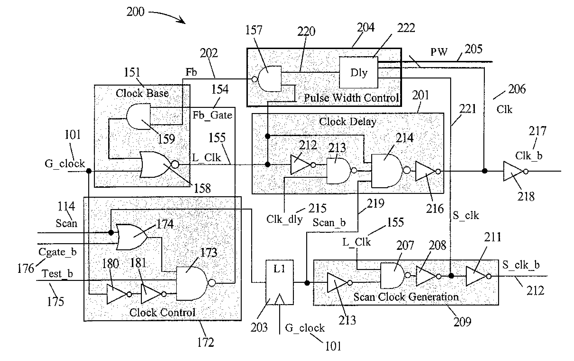
[0024]In the following description, numerous specific details are set forth to provide a thorough understanding of the present invention. For example, specific logic functions and the circuitry for generating them may be described; however, it would be recognized by those of ordinary skill in the art that the present invention may be practiced without such specific details. In other instances, well-known circuits have been shown in block diagram form in order not to obscure the present invention in unnecessary detail. Refer now to the drawings wherein depicted elements are not necessarily shown to scale and wherein like or similar elements are designated by the same reference numeral by the several views.
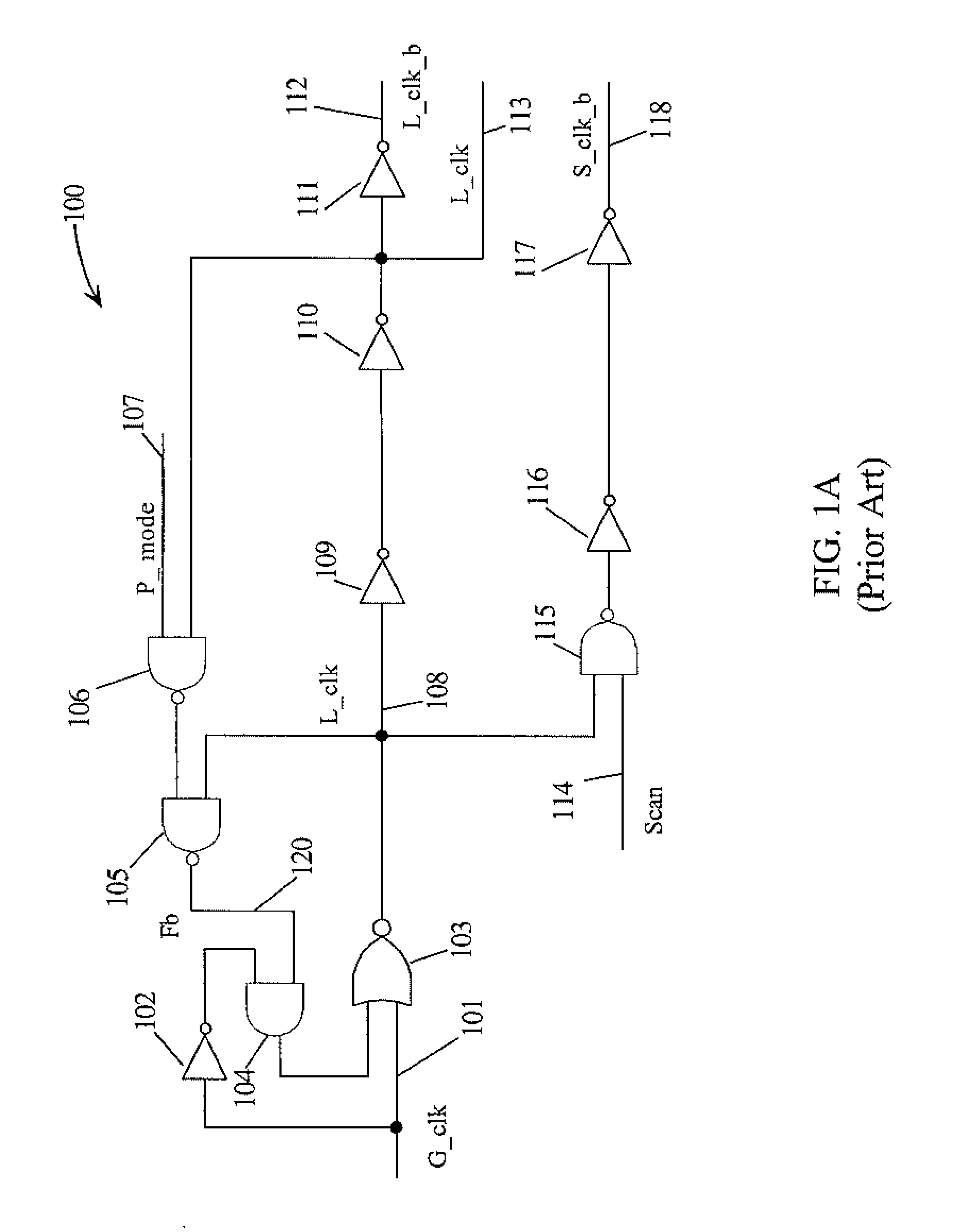
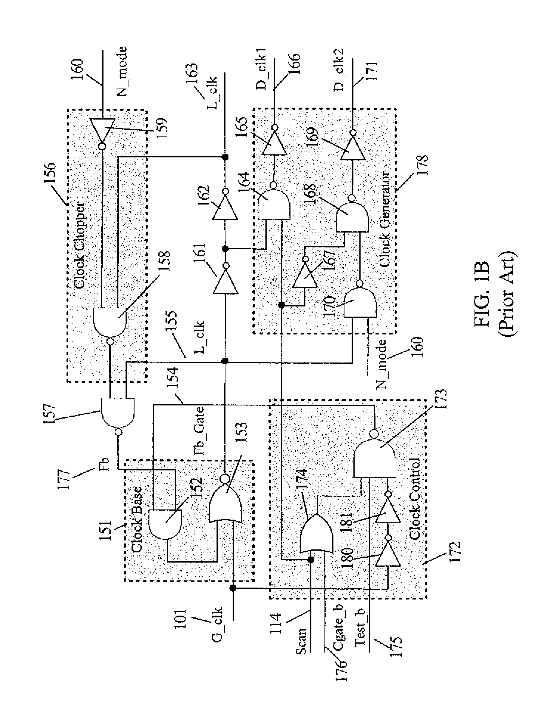
[0025]FIG. 1A is prior art circuitry 100 for generating a pulsed or normal data clock and scan clock. A Global clock, G_clk 101, is received in an exemplary NOR logic gate 103 that has a second input coupled to AND logic gate 104. AND gate 104 has a first input coupled to a feedback...
PUM
 Abstract
Description
Claims
Application Information