Micro thin-film structure, MEMS switch employing such a micro thin-film, and method of fabricating them

a micro-thin-film structure and switch technology, applied in relays, generators/motors, instruments, etc., can solve the problems of insufficient effect of preventing the deformation of the movable electrode, easy bending of the movable electrode, and insufficient lamination structure, so as to improve the lamination structure and reduce the deformation of the thin-film structure

Inactive Publication Date: 2010-06-29
SAMSUNG ELECTRONICS CO LTD
View PDF14 Cites 2 Cited by
  • Summary
  • Abstract
  • Description
  • Claims
  • Application Information

AI Technical Summary

Benefits of technology

[0014]Accordingly, the present invention has been made to solve the above-mentioned problems, and an object of the present invention is to provide a micro thin-film structure improved in lamination structure to reduce the deformation of the thin-film structure.
[0015]A second object of the present invention is to provide a MEMS switch improved in lamination structure of a movable electrode of the MEMS switch to reduce the deformation of the movable switch, so that the movable electrode can perform stable switching operation.
[0016]A third object of the present invention is to provide a method of manufacturing a micro thin-film structure, which improves step of laminating a thin-film of the micro thin-film structure to reduce the deformation of the thin-film structure.
[0017]A fourth object of the present invention is to provide a method of manufacturing a MEMS switch, which includes a step of laminating a thin film of a movable electrode of the MEMS switch to reduce the deformation of the movable electrode, so that the movable electrode can perform stable switching operation.

Problems solved by technology

However, there is a problem in that because the length L of the movable electrode 6 is relatively very large as compared to the distance d between the movable electrode 6 and the substrate 2, the movable electrode 6 is easily bent.
Therefore, there is a problem in that the effect of preventing the deformation of the movable electrode is insufficient.
Such deformation of a thin film structure may cause a problem not only in the above-mentioned MEMS switch but also in other devices employing MEMS techniques.

Method used


Image

  • Micro thin-film structure, MEMS switch employing such a micro thin-film, and method of fabricating them
  • Micro thin-film structure, MEMS switch employing such a micro thin-film, and method of fabricating them
  • Micro thin-film structure, MEMS switch employing such a micro thin-film, and method of fabricating them

Examples


Embodiment Construction

[0047]Hereinbelow, the exemplary embodiments of the present invention will be described in more detail with reference to the accompanying drawings.

[0048]The matters defined in the description such as a detailed arrangement and elements are nothing but the ones provided to assist in a comprehensive understanding of the invention. Thus, it is apparent that the present invention can be carried out without those defined matters. Also, well-known functions or arrangements in the art are not described in detail since they would unnecessarily obscure the invention. Further, the constructions shown in accompanying drawings are depicted in an enlarged scale as compared to practical sizes thereof.

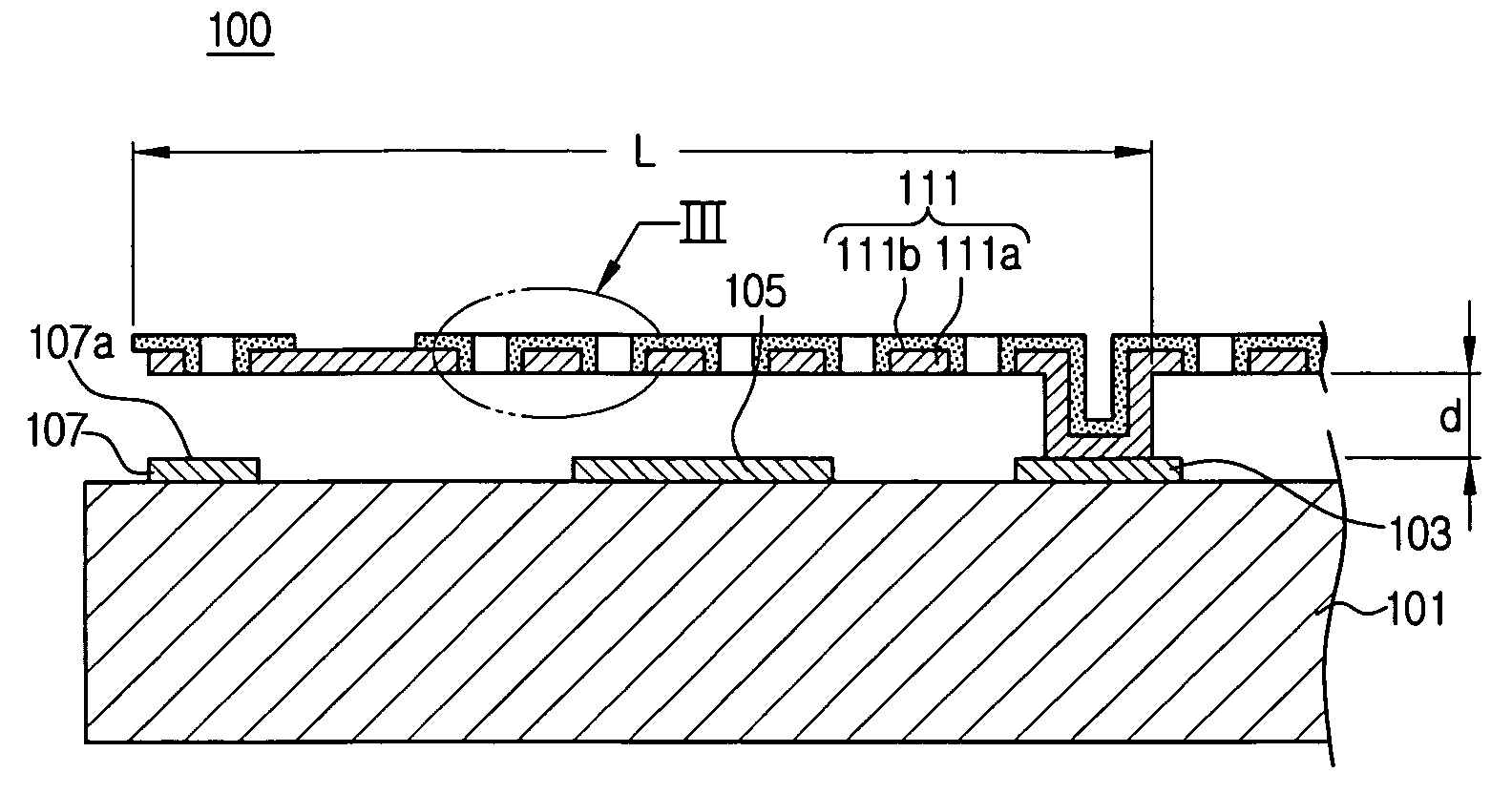
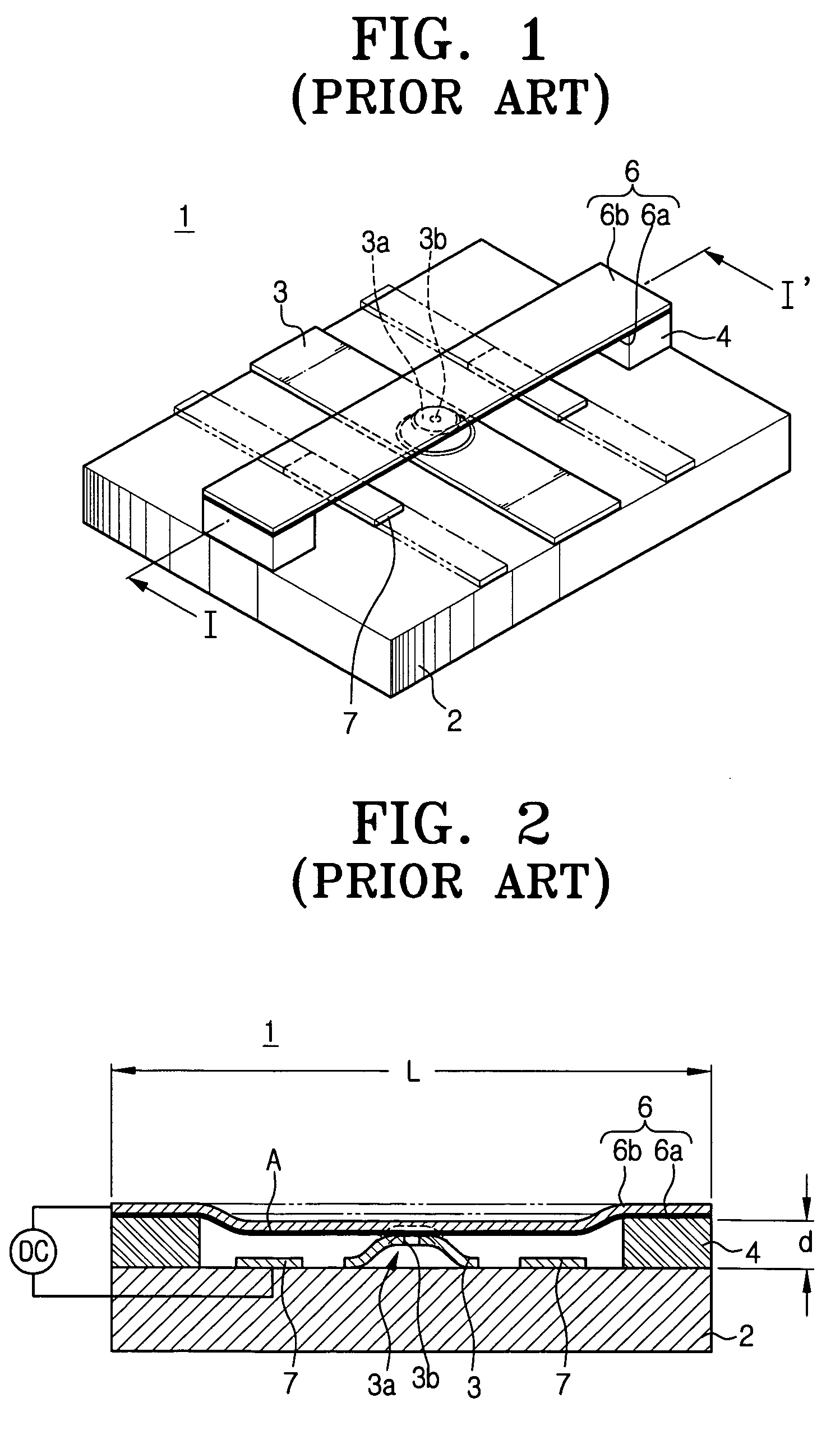
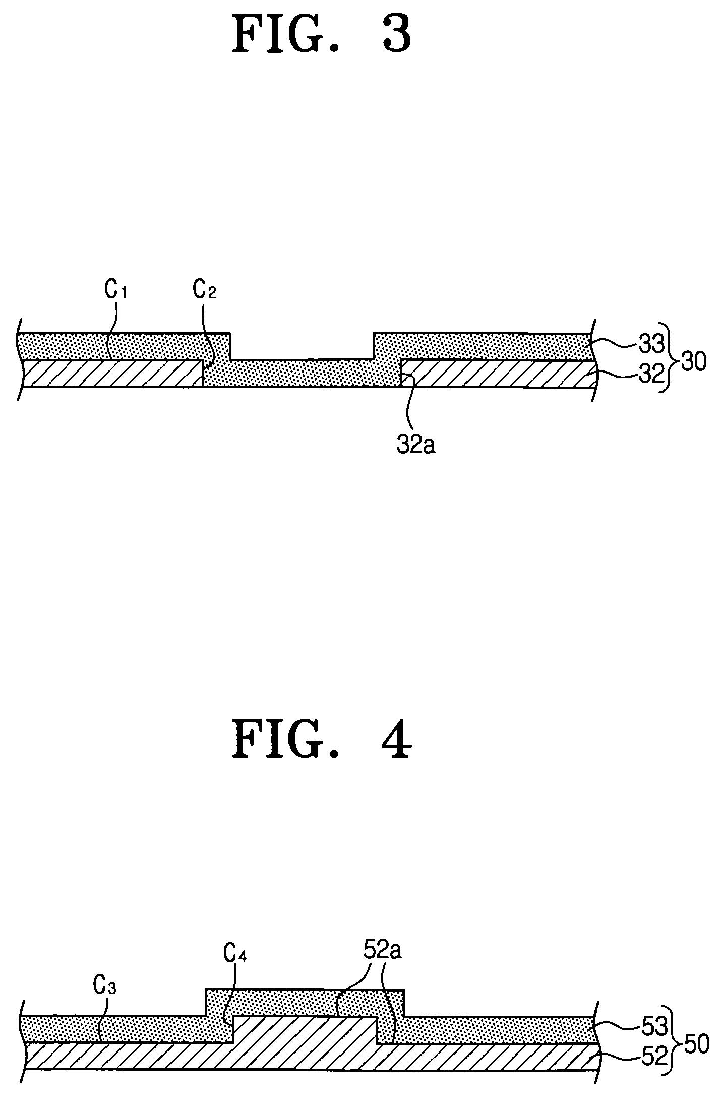
[0049]The inventive micro thin-film structure has two thin-films different in physical property and deposited in sequence to form upper and lower layers, wherein the interface between the upper and lower layers are formed to be oriented to two directions so as to minimize the deformation of the thin-...


PUM


Abstract

A micro thin-film structure, a micro electro-mechanical system (MEMS) switch, and methods of fabricating them. The micro thin-film structure includes at least two thin-films having different properties and laminated in sequence to form an upper layer and a lower layer, wherein an interface between the upper and lower layers is formed to be oriented to at least two directions. The micro thin film structure, and method of forming, may be applied to a movable electrode of an MEMS switch. The thin-film structure may be formed by forming through-holes in the lower layer, and depositing the upper layer in the form of being engaged in the through-holes. Alternatively, the thin-film structure may be made by forming prominence and depression parts on the top side of the lower layer and then depositing the upper layer on the top side of the lower layer having the prominence and depression parts.

Description

CROSS-REFERENCE TO RELATED APPLICATIONS[0001]This application claims priority from Korean Patent Application No. 2004-86056, filed on Oct. 27, 2004, in the Korean Intellectual Property Office, the disclosure of which is incorporated herein by reference.BACKGROUND OF THE INVENTION[0002]1. Field of the Invention[0003]The present invention relates to a micro thin-film structure, a MEMS (Micro Electro-Mechanical System) switch employing such a micro thin-film structure, and methods of fabricating the micro thin-film structure and the MEMS switch, and in particular to a micro thin-film structure, which is improved in lamination structure to minimize the deformation of the micro thin-film structure and allows a MEMS switch to be stably operated when the micro thin-film structure is applied to a movable electrode of the MEMS switch, a MEMS switch employing such a micro thin-film structure, and methods of fabricating them.[0004]2.Description of the Related Art[0005]Among RF devices fabricat...

Claims


Application Information

Patent Timeline
Patent Type & Authority Patents(United States)
IPC IPC(8): G02B26/00H02N2/00
CPCH01H1/0036H01H59/0009B81B3/00B81B7/02
Inventor KWEON, SOON-CHEOLSHIN, HYUNG-JAEJEON, BYUNG-HEEHONG, SEOK-KWANKIM, CHE-HEUNGLEE, SANG-HUN
Owner SAMSUNG ELECTRONICS CO LTD
Why Eureka
Try Eureka