
Photonic sensors, xerogel-based sensors and nanosensors

a photonic sensor and nanosensor technology, applied in the field of analyte detection, can solve the problems of electrical power limit of any photonic sensor device, and achieve the effects of reducing error, improving reliability, and reducing power limi

Inactive Publication Date: 2010-07-06
THE RES FOUND OF STATE UNIV OF NEW YORK
View PDF3 Cites 19 Cited by
  • Summary
  • Abstract
  • Description
  • Claims
  • Application Information

AI Technical Summary

Benefits of technology

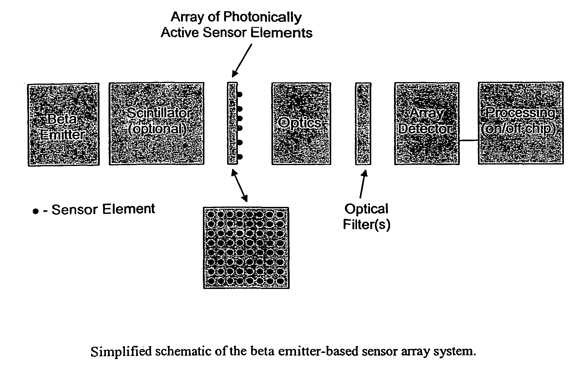
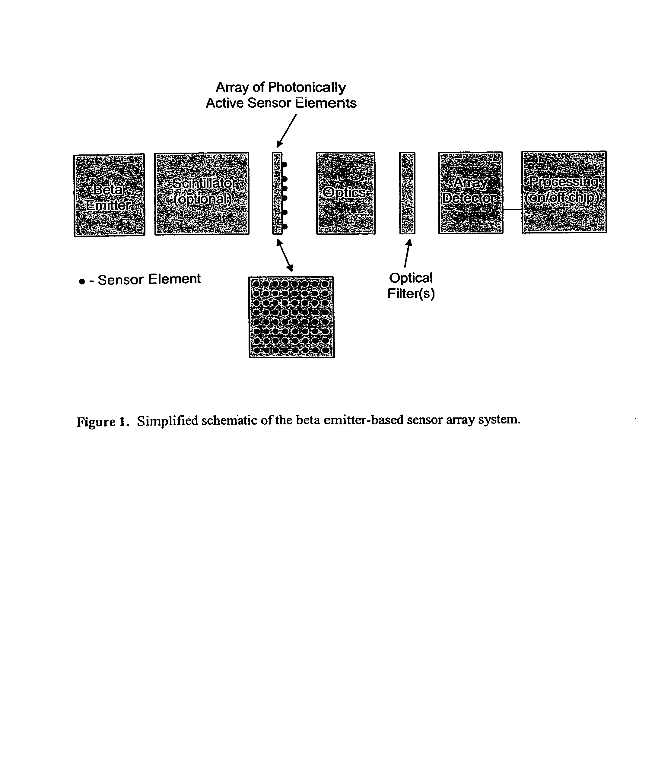
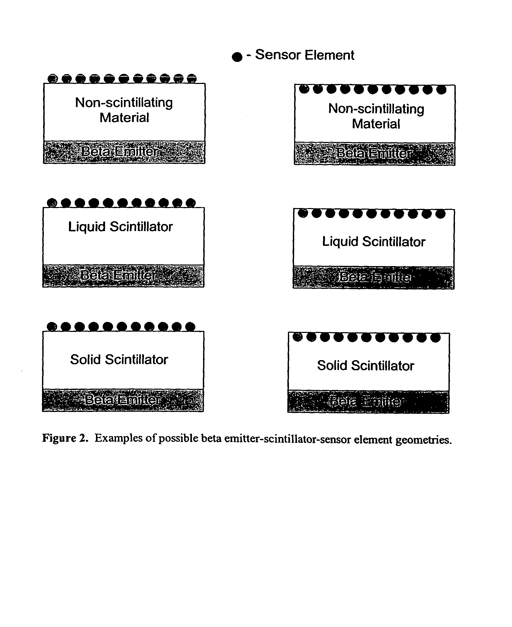
[0007]The present invention provides a photonic sensor system for the detection of, and in one embodiment, the two dimensional resolution of, a chemical analyte. It functions by measuring the radiation from sensors which are in contact with a sample. The sensors are stimulated to radiate either by a beta emission source or a by radiation from a scintillation layer which is interposed between a beta emission source and the sensor. During exposure of the sensors to the desired analyte, the radiation from the sensor changes in intensity, wavelength or both. By comparing the radiation during analyte exposure to the radiation from the sensor unexposed to the analyte, the concentration of analyte in a sample can be determined. If a sensory array is used, two dimensional resolution of concentration can be determined. Distributions of sensors can be used to give an “image” of analyte in a sample. If a sensory array with sensors which are sensitive to multiple different analytes are used, multiple analytes can be simultaneously detected in a sample. Also provided are sensory arrays which have increased reliability and lower error than existing sensors due to the use of an array with diversified sensors for a single analyte.
[0008]In general, unlike existing methods, the source of photons which impinge on the sensory array (i.e., the beta emission source, either with or with out a scintillation layer) does not require an external power source, and can remain stable over long periods of time without attention.
[0009]The present invention further provides a method for preparing sensory arrays which allow greater spatial resolution than previously attainable. The method comprises the creation of pin printing arrays in which the pins have been created from specific materials by pulling, cutting or etching, optionally followed by the treatment of the pin tips with materials which allow the easy dispensing of ultra-small array sensors.

Problems solved by technology

This need for electrical power limits any photonically-based sensor device.

Method used


Image

  • Photonic sensors, xerogel-based sensors and nanosensors
  • Photonic sensors, xerogel-based sensors and nanosensors
  • Photonic sensors, xerogel-based sensors and nanosensors

Examples


example 1

[0117]The unique nature of the beta emission yields several possible data formats from the CRNILS (FIG. 10). In FIG. 10A, results are presented where the luminescence spectrum from the sensing layer shifts in the presence of the target analyte. Potential calibration curves are presented in FIG. 11A. Curves 1-3 in FIG. 11A represent different sensing chemistries / sensing layer formulations for the same target analyte-diversification. In FIG. 10B, results are presented where the luminescence intensity from the sensing layer changes in the presence of the target analyte. Potential calibration curves are presented in FIG. 11B. Curves 1-3 in FIG. 11B represent different sensing chemistries / sensing layer formulations for the same target analyte-diversification. In FIG. 10C, results are presented where the time-resolved intensity decay profiles of the sensing layer change in the presence of the target analyte. Potential calibration curves are presented in FIG. 11C. Curves 1-3 in FIG. 11C re...

example 2

[0118]FIG. 14 presents examples of pin printed microarrays that have been formed in the laboratory. The printing solution was a 50:50 mole % tetramethylorthosilane:n-octyl-trimethoxysilane-based xerogel doped with the fluorophore rhodamine 6G.

[0119]The arrays are illuminated with a laser in an epi-fluorescence geometry, detection is with a CCD camera. The “Pulled fiber” array was formed from a single fused silica optical fiber (geometry, round, solid, points in FIG. 12). The printed feature sizes are 14±3 micrometers in diameter. Arrays are also shown for commercial quill and solid pins. In all cases, the feature size with the commercial pins is at least an order-of-magnitude larger in diameter when compared to our “Pulled fiber”. The pulled fiber can be used to increase the printed element density by ˜100×).

example 3

[0120]Inspection of Eqn. 1 reveals two strategies for tuning the sensitivity of any quenchometric sensor—adjust τ0 and / or adjust kq. (Note; In other sensor schemes one might tune the binding affinity, partition coefficient, etc. to generate the necessary sensor diversity.)

[0121]To illustrate the potential of this tuning we formed a diversified library of xerogel-based sensor elements for O2. Here, each sensor element is designed so that it exhibits a distinct calibration curve and / or response time course to dissolved or gaseous O2. In this particular example, these diversified xerogel-based photonic sensor libraries are derived from luminophore-doped xerogels. The xerogels are composed of n-alkyl (C1-C12)-triethoxysilane (C1-C12)-TriEOS) and tetraethoxysilane (TEOS) or n-alkyl (C1-C12)-trimethoxysilane (C1-C12)-TriMOS) and tetramethyoxysilane (TMOS) precursors. The luminophores are tris(4,7-diphenyl-1,10-phenanthroline)ruthenium(ll), [Ru(dpp)3]2+ and / or tris(2,2′-bipyridyl)ruthenium...


PUM

PropertyMeasurementUnit
diameteraaaaaaaaaa
sizeaaaaaaaaaa
sizesaaaaaaaaaa

Abstract

A photonic sensor system is provided. The system generally includes a beta emission source, optionally, a scintillation layer, and a luminophore-containing sensory layer. The system can be embodied in a particle. Also provided are photonic sensor strategies which are highly accurate and photonic sensors which are highly stable.

Description

[0001]This application claims priority to Provisional Application No. 60 / 551,818, filed on Mar. 10, 2004.[0002]This invention was made with Government support under grant numbers CHE-0315128 from the National Science Foundation (NSF) and N00014-02-1-0836 from the Office of Naval Research (ONR). The Government has certain rights in the invention.FIELD OF THE INVENTION[0003]The present invention relates generally to area of detection of analytes.BACKGROUND[0004]The desire to simultaneously measure “everything” in any sample has driven the development of artificial “noses” and “tongues”. These devices have been based on a wide variety of sensor array strategies. Examples of sensor arrays include those based on cantilevers, conducting polymers, electrochemistry, photonics, the piezoelectric effect, or surface acoustic waves. In a photon-based sensor, one requires a photon source, appropriate sensing chemistry (i.e., a recognition element), a means to immobilize the desired sensing chemi...

Claims


Application Information

Patent Timeline
Patent Type & Authority Patents(United States)
IPC IPC(8): G01N21/00
CPCG01N21/6408G01N21/6428G01N21/6452G01N2021/6432G01N2021/7786G01N2201/061G01N2201/06193
Inventor BRIGHT, FRANK V.HOLTHOFF, WILLIAM G.TEHAN, ELIZABETH C.
Owner THE RES FOUND OF STATE UNIV OF NEW YORK
Learn More