
LED structure and fabricating method for the same

a technology of led structure and fabrication method, which is applied in the direction of discharge tube luminescnet screen, discharge tube/lamp details, electric discharge lamps, etc., can solve the problems of deteriorating the luminescent efficiency of led, the decay rate of dies, and the discovery of great difficulties, so as to enhance the uniformity of light, avoid dispersion, and uniform white light

Inactive Publication Date: 2010-07-13
EDISON-OPTO
View PDF8 Cites 4 Cited by
  • Summary
  • Abstract
  • Description
  • Claims
  • Application Information

AI Technical Summary

Benefits of technology

[0007]In the light of the foregoing drawbacks, the present invention is to provide an LED fabrication method and its structure that is able to produce uniform white light. The realization of the method and its structure is by laying a hollow holding frame on top of an LED die, filling the holding frame with yellow fluorescent substance and making the substance uniformly cover the die. Once blue light emitted by the die excites the yellow fluorescent substance, a uniform white light can then be produced. This approach can not only enhance the uniformity of light and avoid dispersion, but also improve accuracy and precision during its fabrication process.

Problems solved by technology

Even though the technique has good luminescent efficiency, the difference in current control and variations in decay rate of dies surely deteriorate the luminescent efficiency of the LED.
Therefore, there are unexpected factors embedded in the foregoing art, and great difficulties are surely found once in carrying out the manufacturing.

Method used


Image

  • LED structure and fabricating method for the same
  • LED structure and fabricating method for the same
  • LED structure and fabricating method for the same

Examples


Embodiment Construction

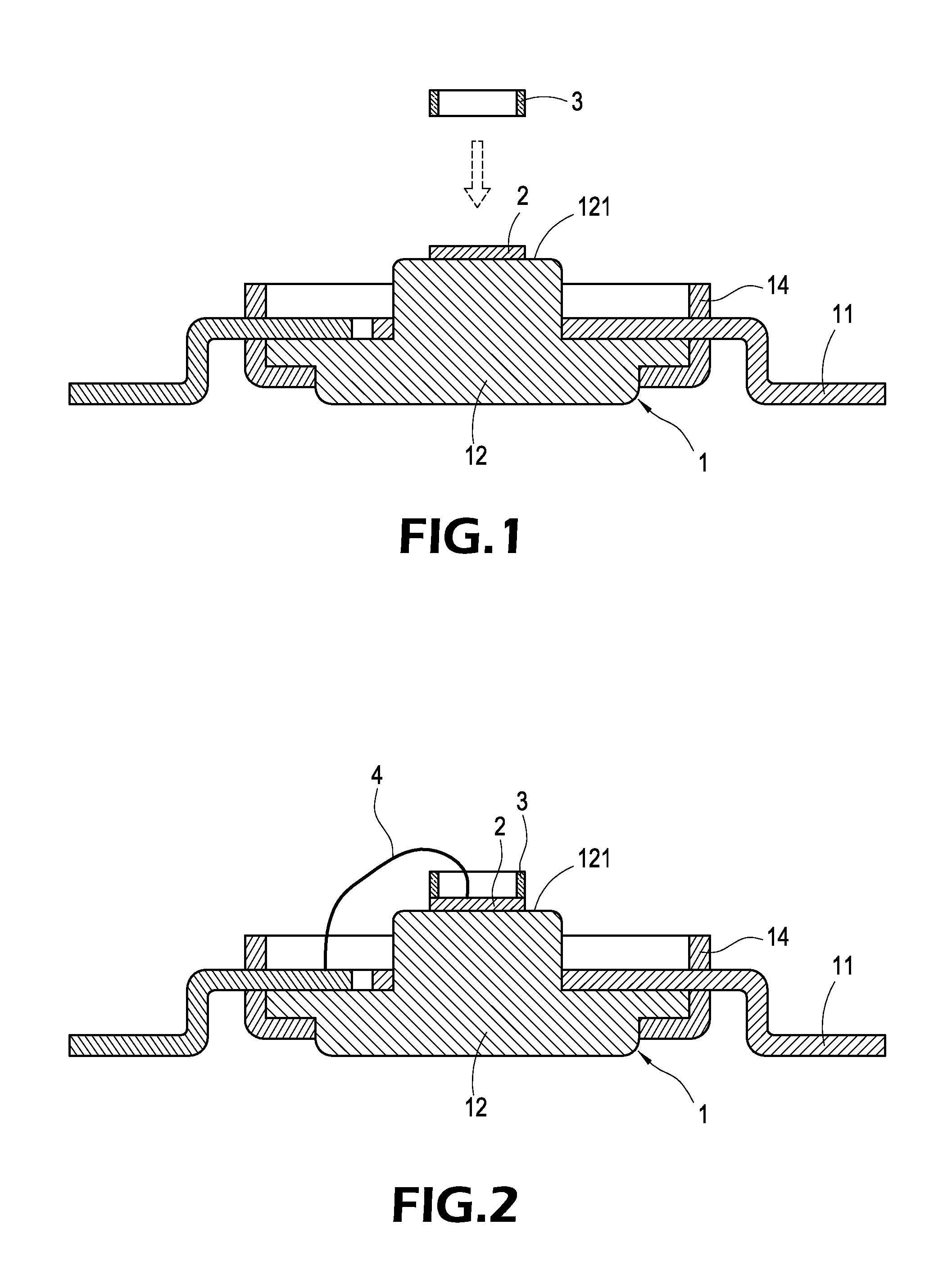
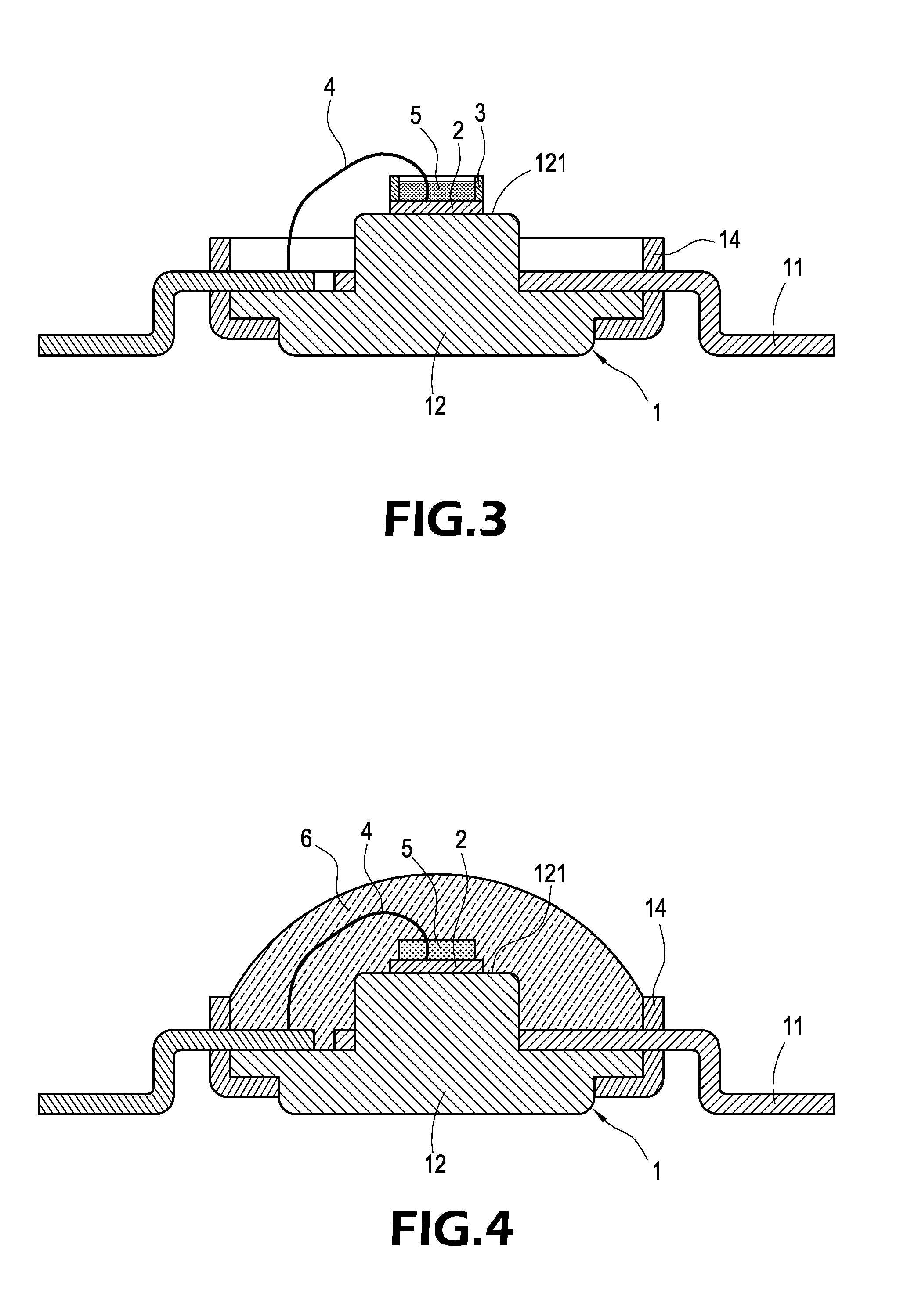
[0019]The drawings, FIG. 1 through FIG. 4, are cross-sectional views that show the preferred embodiment of the LED packaging process according to the present invention. Referring to FIG. 1, the LED structure according to the LED packaging process of the present invention comprises an LED substrate 1, an LED die 2, and a holding frame 3. The LED substrate 1 of the embodiment is a semi-finished frame-type LED, where the substrate 1 further comprises a frame 11 for providing electric conduction and a heat sink 12, and is encapsulated by the injected heat-resisting plastic to form an encapsulation 14. The heat sink 12 of the LED substrate 1 has a planar surface 121 that is devised for the LED die 2. The LED die 2 is capable of emitting blue light. A holding frame 3 is laid on the die 2 and attaches to the die 2 after the die 2 was bonded on top of the planar surface 121. The holding frame 3 is of hollow shape and embraces an area dimension smaller than the area of the die 2. The frame 3...


PUM


Abstract

A method is performed for the fabrication of LED and its structure. The LED is capable of emitting uniform white light and includes a substrate, an LED die, a holding frame and fluorescent substance where the holding frame is of hollow shape. The LED contains a die emitting blue light, and the fluorescent substance is a yellow phosphor. As the LED die is mounted on the substrate, the holding frame is seated on the die, and a bond wiring is performed. The holding frame is filled with the fluorescent substance in a uniform distribution on the die to form a layer of fluorescence. Finally the structure of the LED is accomplished as the packaging is completed.

Description

BACKGROUND OF THE INVENTION[0001]1. Field of the Invention[0002]The present invention relates to a light emitting diode (LED) and more particularly to a method for fabricating the LED and the structure thereof.[0003]2. Description of the Prior Art[0004]LED is a solid-state semiconductor device, which makes use of the recombination of two charged carriers by electrical current flowing through a diode, to release energy in the form of light, featuring advantages of compact in size, fast response, and high efficiency. Therefore LED has versatile applications to a variety of industries.[0005]Due to its compact size, LED can be used for various applications. For example, the LED has gained great popularity for lighting application. Moreover, the demand for white LED has been substantially boosted. White light is produced by blending multiple colors in the visual spectrum. The white light visible to the human eyes is formed by mixing at least two colors of different wavelengths in appropr...

Claims


Application Information

Patent Timeline
Patent Type & Authority Patents(United States)
IPC IPC(8): H01J1/62H01J63/04
CPCH05B33/10H05B33/145H05B33/22H01L2224/48091H01L2224/48247H01L2224/8592H01L2924/00014
Inventor SUN, TSUNG-TINGLAIO, HUNG-TACHOU, HUNG-HSUNHSU, KUO-SHIHCHEN, PAO-SHEN
Owner EDISON-OPTO
Learn More