Semiconductor light emitting module and method of manufacturing the same

a technology of semiconductor light emitting modules and light-emitting modules, which is applied in the direction of semiconductor devices for light sources, light and heating apparatus, planar light sources, etc., can solve the problems of preventing the creation of a lightweight semiconductor light-emitting module and the ineffective heat dissipation from the front surface, and achieves a high reflection coating

Inactive Publication Date: 2013-05-02
S E I INC +1
View PDF15 Cites 1 Cited by
  • Summary
  • Abstract
  • Description
  • Claims
  • Application Information

AI Technical Summary

Benefits of technology

[0008]An object of the present invention is to provide a semiconductor light emitting module and a method of manufacturing the same, which allow maintaining higher reflectivity, obtaining uniform white light, achieving high luminance light emission by improving light extraction efficiency, while having lightweight and thin features.

Problems solved by technology

Hence there is a drawback that heat dissipation from the front surface cannot be effectively performed.
This prevents creating a lightweight semiconductor light emitting module.

Method used


Image

  • Semiconductor light emitting module and method of manufacturing the same
  • Semiconductor light emitting module and method of manufacturing the same
  • Semiconductor light emitting module and method of manufacturing the same

Examples


first embodiment

(A Structure Of A Semiconductor Light Emitting Module)

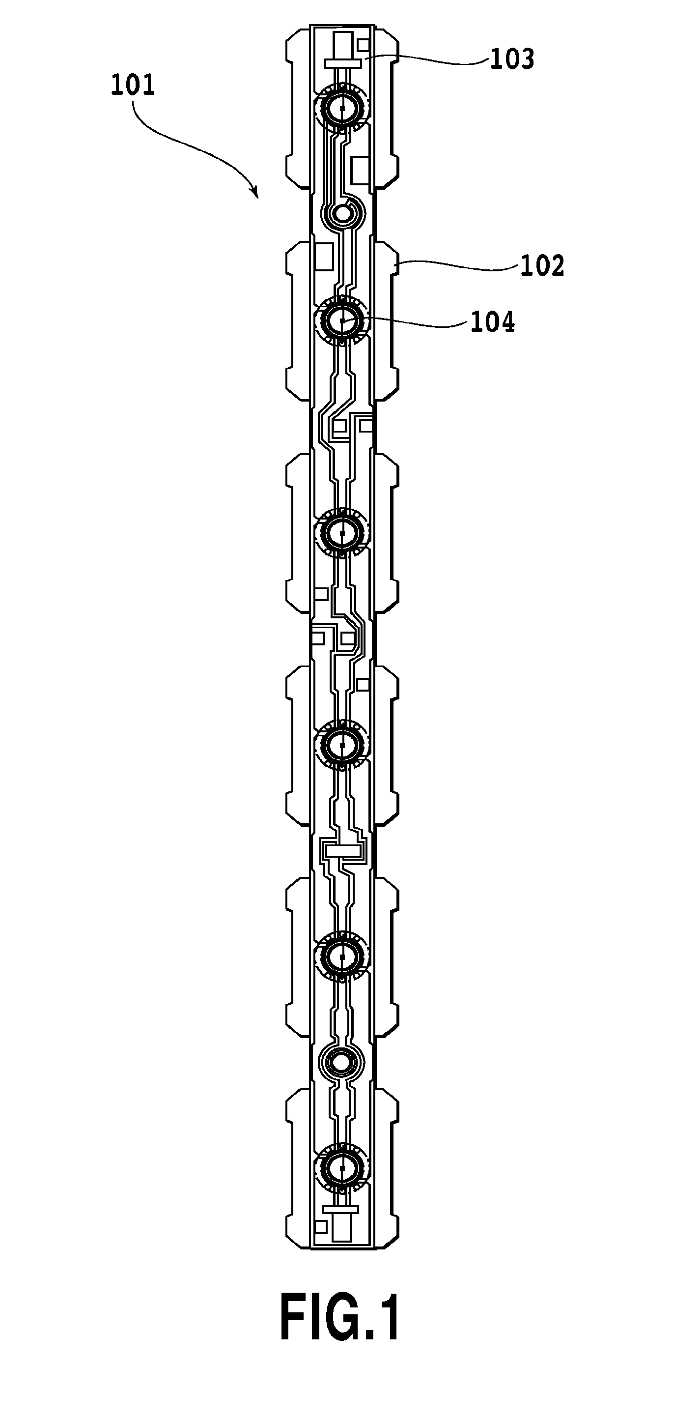
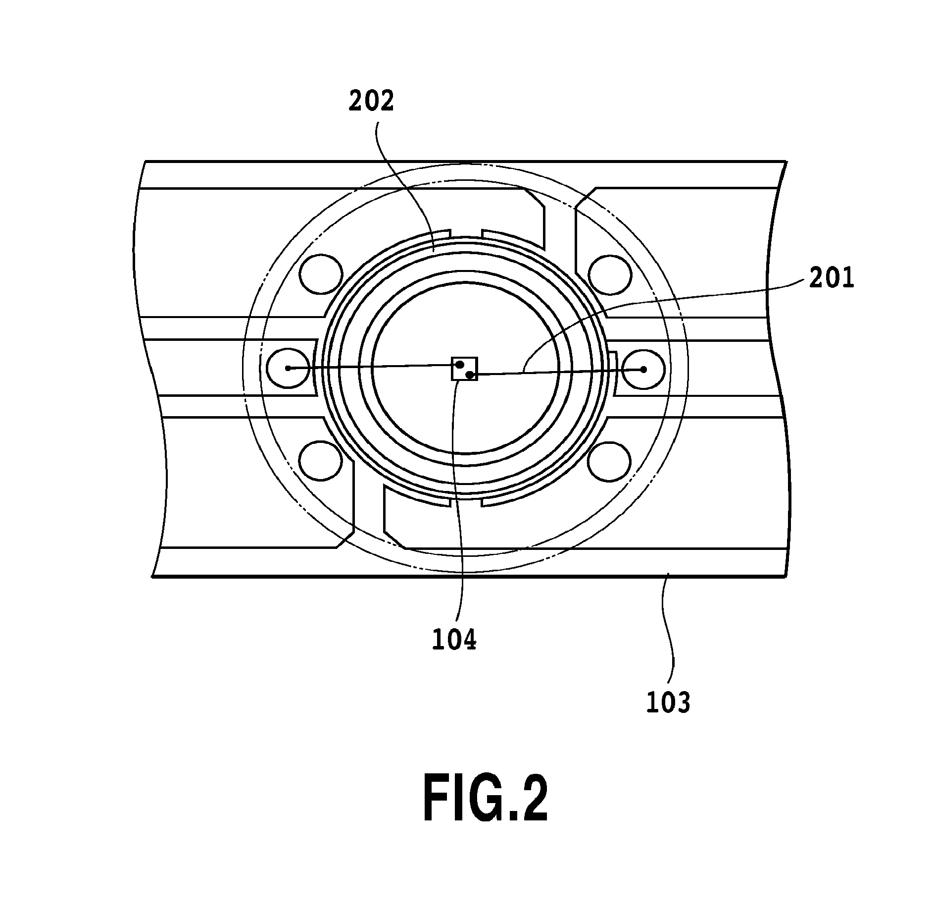
[0059]FIG. 1 is a top view showing a structure of a semiconductor light emitting module according to an embodiment of the present invention. A semiconductor light emitting module 101 of this embodiment includes metal thin plates 102 configured to dissipate heat and provided with a light reflecting function, and a printed board 103 configured to cover the metal thin plates 102 and to supply electric power to semiconductor light emitting elements 104 disposed on the metal thin plates. The semiconductor light emitting elements 104, such as light-emitting diodes, to be actually energized to emit light are electrically connected to the printed board 103. In this embodiment, the printed board 103 is formed into a vertically long shape as shown in FIG. 1, and the metal thin plates 102 are attached thereto in an array form. Here, as can be understood by referring to FIG. 1, the metal thin plates 102 are structurally formed into such shap...

second embodiment

[0086]FIGS. 14A and 14B are a front view and a lateral side view showing a structure of an example of a semiconductor light emitting module according to this embodiment. As similar to the above-described first embodiment, a semiconductor module of this embodiment similarly forms therein the projecting portion 202 serving as the reflecting member on the metal thin plate 102 in a way that the projecting portion 202 surrounds the semiconductor light emitting element 104, and connects the semiconductor light emitting element 104 to the printed board 103 by using the wire 201 or the like, for example, but is different in that a high reflection paint portion 1401 is provided at a gap portion between the printed board covering the metal thin plate 102 and the projecting portion 202 as shown in FIG. 14B.

[0087]Specifically, the printed board 103 having an opening for the projecting portion 202 is formed so as to be stacked on the metal thin plate 102 in the first embodiment. Here, as can be ...

third embodiment

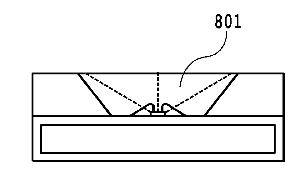
[0092]FIGS. 15A and 15B are a front view and a lateral side view showing a structure of an example of a semiconductor light emitting module according to this embodiment. The semiconductor module of this embodiment is similar to the above-described second embodiment in that the a high reflection paint portion 1501 is provided at an edge portion of an opening of the printed board 103 to cover the metal thin plate 102 and is different from the second embodiment in that the metal thin plate 102 does not include the projecting portion 202 serving as the reflecting member provided so as to surround the semiconductor light emitting element 104.

[0093]Specifically, in the second embodiment, the printed board 103 having an opening for the projecting portion 202 is formed to be stacked on the metal thin plate 102 and the inclined surface of the projecting portion 202 plays a role as a reflecting plate to increase reflection efficiency. Meanwhile, as can be understood by referring to the latera...


PUM


Abstract

Provided are a semiconductor light emitting module and a method of manufacturing the same, which allow achieving high luminance light emission as well as lightweight and compact features. In a semiconductor light emitting module (101), a projecting portion (202) serving as a reflecting member is formed on a metal thin plate (102) to surround a semiconductor light emitting element (104). The semiconductor light emitting element (104) is connected to a printed board (103) by using a wire (201), for example. The projecting portion (202) is formed by pressing and bending the metal thin plate (102) from a back surface, for example, to surround the element and to be higher than the semiconductor light emitting element (104).

Description

CROSS-REFERENCE TO RELATED APPLICATIONS[0001]This Application is a divisional of U.S. patent application Ser. No. 12 / 934,533 filed on Dec. 21, 2010, which is a National Stage of International Application No. PCT / JP2009 / 055517, which claims the benefit of Japanese Patent Application No. 2008-081716 filed on Mar. 26, 2008, all of which are incorporated herein by reference in their entirely.TECHNICAL FIELD[0002]The present invention relates to a semiconductor light emitting module and a method of manufacturing the same, or more specifically, to a semiconductor light emitting module and a method of manufacturing the same which enable high luminance light emission.BACKGROUND ART[0003]In recent years, semiconductor light emitting elements such as light emitting diodes (LED) having high energy efficiency in light emission have been used in various fields, and various apparatuses utilizing such semiconductor light emitting elements have been developed. Emitting light with large currents or ...

Claims


Application Information

Patent Timeline
Patent Type & Authority Applications(United States)
IPC IPC(8): H01L33/60H01L33/48
CPCH01L25/0753H01L33/483H01L33/644H05K2203/0323H05K2201/10106H01L33/60H01L33/641H01L2224/48091H01L2224/48247H01L2224/8592F21K9/00F21Y2101/02F21Y2105/001H01L33/62H01L33/642H05K1/021H05K2201/09054H01L2924/00H01L2924/00014F21Y2105/10F21Y2115/10H01L2924/181F21Y2105/16H01L2924/00012H01L33/48
Inventor KOMATSUBARA, SATOSHIFUKUDA, KENICHIOTAO, SHINOBUFURUTA, TORU
Owner S E I INC
Why Eureka
Try Eureka