Surface emitting semiconductor laser

a semiconductor laser and surface technology, applied in semiconductor lasers, laser details, electrical equipment, etc., can solve the problem of less than the desired value of the reflection of the mirror

Inactive Publication Date: 2000-04-18
II VI LASER ENTERPRISE
View PDF2 Cites 106 Cited by
  • Summary
  • Abstract
  • Description
  • Claims
  • Application Information

AI Technical Summary

Benefits of technology

A general object of the present invention is to enable surface emitting semiconductor lasers having qualities desired for such lasers to be fabricated economically. A more particular object of the invention is to enable the top mirrors of such lasers to be given both high reflectance and low electrical resistance, particularly for the purpose of emitting light at wavelengths associated with indium phosphide.
In addition, when a semiconductor substrate with N-type doping has a dielectric layer mirror to constitute the bottom mirror of a surface emitting laser formed on said substrate, the present invention makes it possible for the top mirror of the laser to be made in the form of a semiconductor layer mirror having N-type doping and thus obtain the advantages that result from the electrical and optical characteristics associated with this type of doping.

Problems solved by technology

However, passing the current through the top mirror presents a problem when making the mirror.
Unfortunately, reflectance then has a maximum of about 97% and as a general rule that is insufficient.
Those second and third known lasers suffer in particular from the drawback of the semiconductor materials which constitute the top mirror absorbing the light of the laser to such an extent that the reflectance of the mirror is less than the desired value.
This drawback is a result of the fact that binary semiconductor materials with P doping present an absorption coefficient for said light which is greater than that of materials having N-type doping.

Method used


Image

  • Surface emitting semiconductor laser
  • Surface emitting semiconductor laser
  • Surface emitting semiconductor laser

Examples


Embodiment Construction

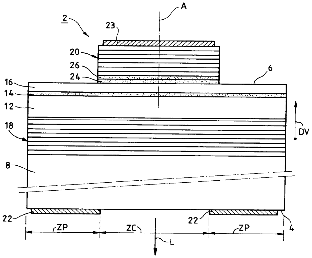
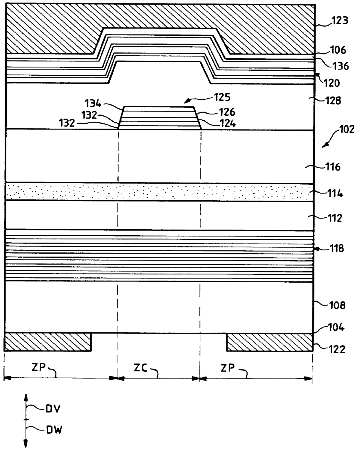
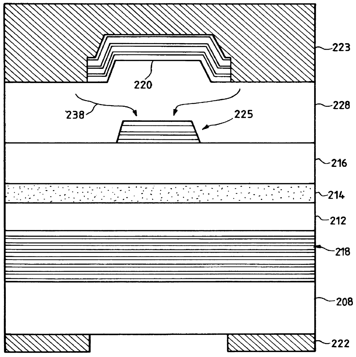
Like the other lasers given by way of example, the chip of the first laser shown in FIG. 1 is constituted by an essentially monocrystalline semiconductor assembly. The assembly is built up by growing a succession of deposits on a substrate. The substrate has an axis A and an area which extends in a plane perpendicular to said axis. Said axis and said area also constitute an axis and an area of said chip. The area has a central zone ZC in the vicinity of the axis A and a peripheral zone ZP around said central zone. The thickness of the chip defines a vertical direction DV parallel to the axis A.

More particularly, the chip 2 of this first laser has a bottom face 4 and a top face 6 and comprises mutually superposed layers. Unless stated otherwise, these layers are made of indium phosphide. Going from the bottom face to the top face, these layers are as follows:

The substrate 8. This substrate is of a thickness giving it mechanical strength enabling the chip to be handled, either on its ...


PUM


Abstract

Two semiconductor layers of the laser form a tunnel junction enabling an electrical current for pumping the laser to pass from an N doped semiconductor Bragg mirror to a P doped injection layer belonging to the light-amplifying structure. The Bragg mirror co-operates with another mirror of the same type having the same doping to include said structure in an optical cavity of the laser. In a variant, the tunnel junction may be buried and located so as to constitute confinement means for said pumping current. The laser can be used in an optical fiber communications network.

Description

The present invention relates to surface emitting semiconductor lasers, i.e. to lasers of the vertical cavity surface emitting laser (VCSEL) type. It enables mirrors to be made that present simultaneously several qualities that are desirable for making the optical cavity of such a laser. The invention is particularly applicable when the light that is to be emitted by such a laser is to have a wavelength in the vicinity of 850 nm, 980 nm, 1300 nm, or 1550 nm so as to be situated in one of the spectral windows commonly used in optical fiber communications systems.In known manner, such light is generated in the active layer of a light-amplifying structure through which there passes a pumping current, and said structure is included in a monocrystalline chip made of a semiconductor material having III-V type binary composition, i.e. gallium arsenide AsGa or indium phosphide InP. Such a chip is fabricated by epitaxially growing layers one on another from a substrate. In the description be...

Claims


Application Information

Patent Timeline
Patent Type & Authority Patents(United States)
IPC IPC(8): H01S5/00H01S5/183H01S5/042
CPCH01S5/18305H01S5/18308H01S2302/00H01S5/3095H01S5/18394
Inventor BRILLOUET, FRANCOISJACQUET, JOELSALET, PAULGOLDSTEIN, LEONGARABEDIAN, PATRICKSTARCK, CHRISTOPHEBOUCART, JULIEN
Owner II VI LASER ENTERPRISE
Why Eureka
Try Eureka