Method of forming non-volatile memory cell
a non-volatile, memory cell technology, applied in semiconductor devices, electrical equipment, semiconductor/solid-state device testing/measurement, etc., can solve the problem of seriously reducing the yield random single bit (rsb) failure rate, chemical damage on the substrate, etc. problem, to achieve the effect of improving the yield, reducing the damage, and reducing the damage to the memory cell
- Summary
- Abstract
- Description
- Claims
- Application Information
AI Technical Summary
Benefits of technology
Problems solved by technology
Method used
Image
Examples
first embodiment
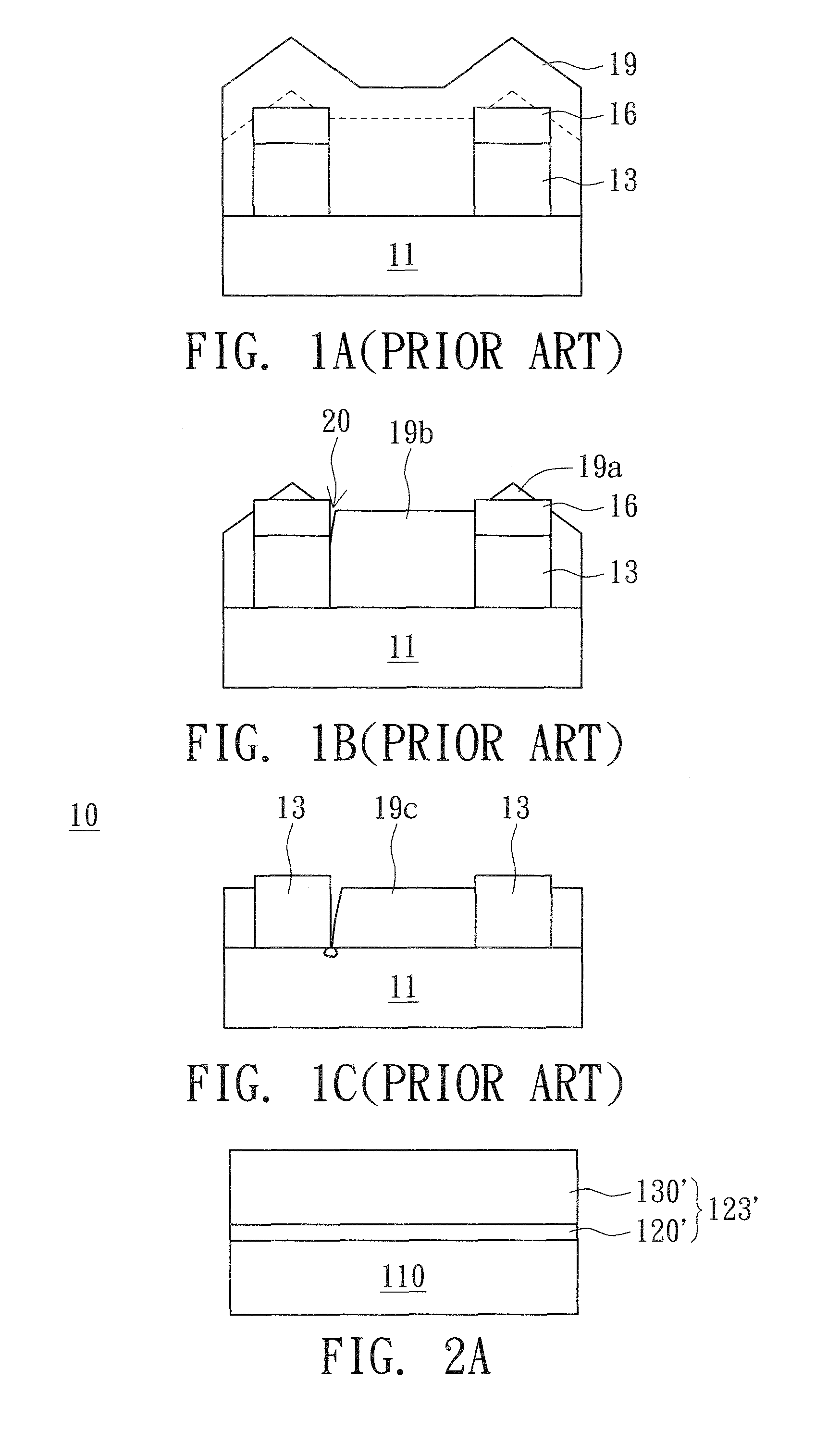
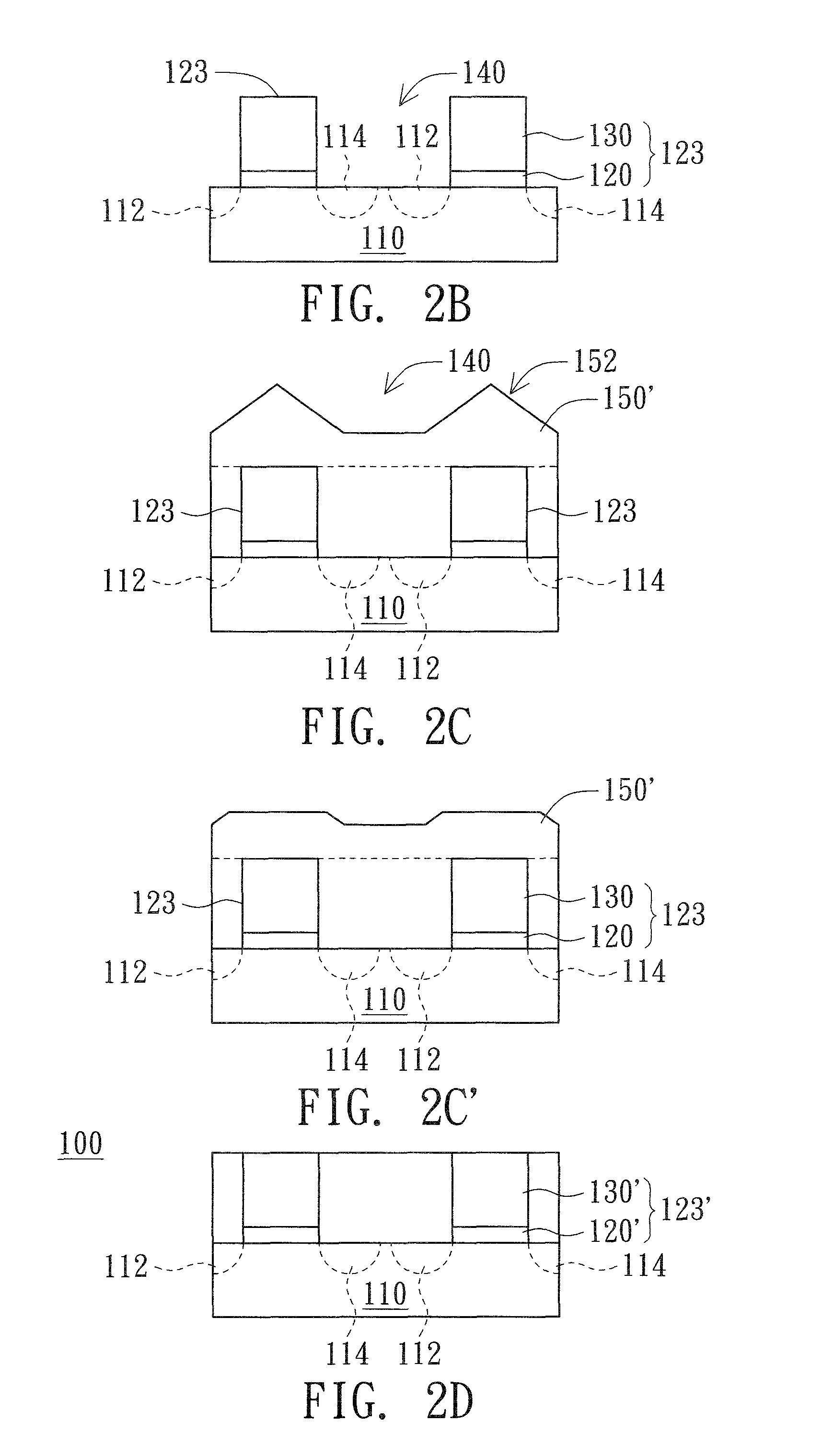
[0015]Referring to FIGS. 2A˜2D, cross-sectional view of diagrams illustrating a method of forming a non-volatile memory cell of the invention according to the first embodiment. The non-volatile memory for example, is read only memory (ROM), programmable read only memory (PROM), erasable programmable read only memory (EPROM), electrically erasable programmable read only memory (EEPROM), flash EEPROM, or nitride trap memory. The method of forming a non-volatile memory cell including following steps. Firstly, a substrate 110 is provided, and a stacking structure 123′ is then formed on the substrate, as shown in FIG. 2A. The stacking structure 123′ at least including an oxide-nitride-oxide (ONO) layer 120′ and a polysilicon layer 130′. The ONO layer 120′ is formed on the substrate 110, and the polysilicon layer 130′ is then formed on the ONO layer 120′. The ONO layer 120′ includes a top oxide layer, a nitride layer, and a bottom oxide layer. The top and the bottom oxide layer are thicke...
second embodiment
[0023]The method of the present embodiment differs from that of the first embodiment in the stopping layer on the top of the stacking structure during the polishing process. The same piece remains numerically labeled the same in the following drawings.
[0024]Referring to FIGS. 3A˜3D, cross sectional views illustrating a method of forming a non-volatile memory cell according to the second embodiment of the invention. Firstly, numerous stacking units 223 are formed on the substrate 110, as shown in FIG. 3A. Besides the ONO layer 120 and the polysilicon layer 130, the stacking units 223 further includes a stopping layer 235 formed on the polysilicon layer 130. Two implantation processes are then be performed to form the source region 112 and drain region 114. The stopping layer 235 is located on the top of the stacking units and blocks accelerating ions during the implantation, so that it prevents the polysilicon layer 130 from being doped. The stopping layer 235 also functions in the f...
PUM
 Abstract
Description
Claims
Application Information


