Method of forming non-volatile memory cell

Active Publication Date: 2008-08-14
MACRONIX INT CO LTD
View PDF9 Cites 0 Cited by
  • Summary
  • Abstract
  • Description
  • Claims
  • Application Information

AI Technical Summary

Benefits of technology

[0009]The invention is directed to a method of forming a non-volatile memory cell, in which the oxide layer between memory cells is planarized by a chemical mechanical polishing process, rather than etched by corrosive acid. Reduced chemical damage on the memory cell contributes to improved random single bit (RSB) failure rate, and it therefore increases the yield.

Problems solved by technology

Chemical damage on the substrate seriously reduces yield random single bit (RSB) failure rate.

Method used


Image

  • Method of forming non-volatile memory cell
  • Method of forming non-volatile memory cell
  • Method of forming non-volatile memory cell

Examples


first embodiment

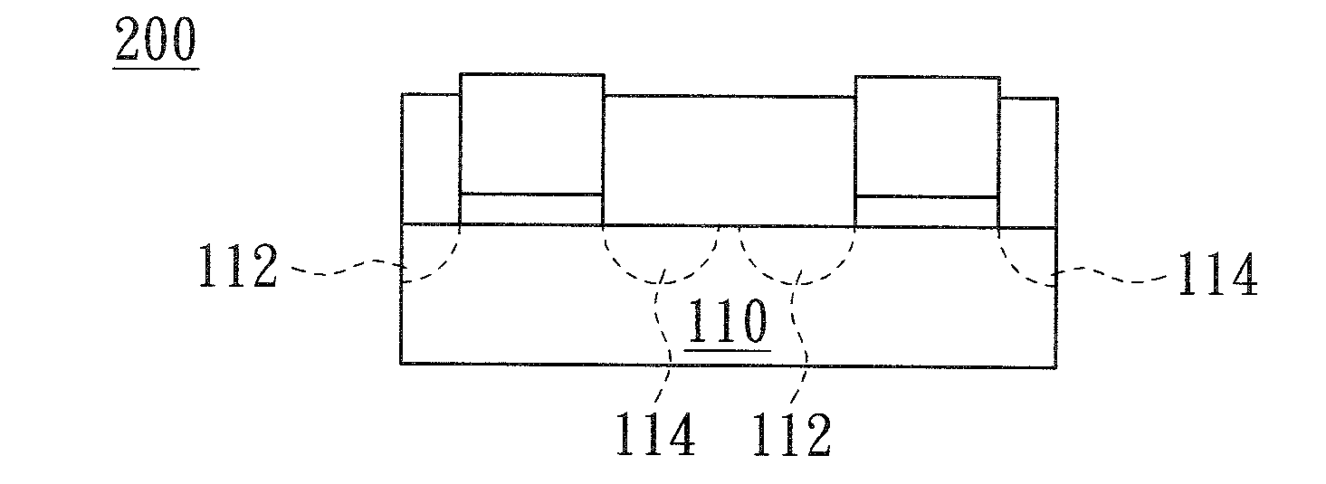
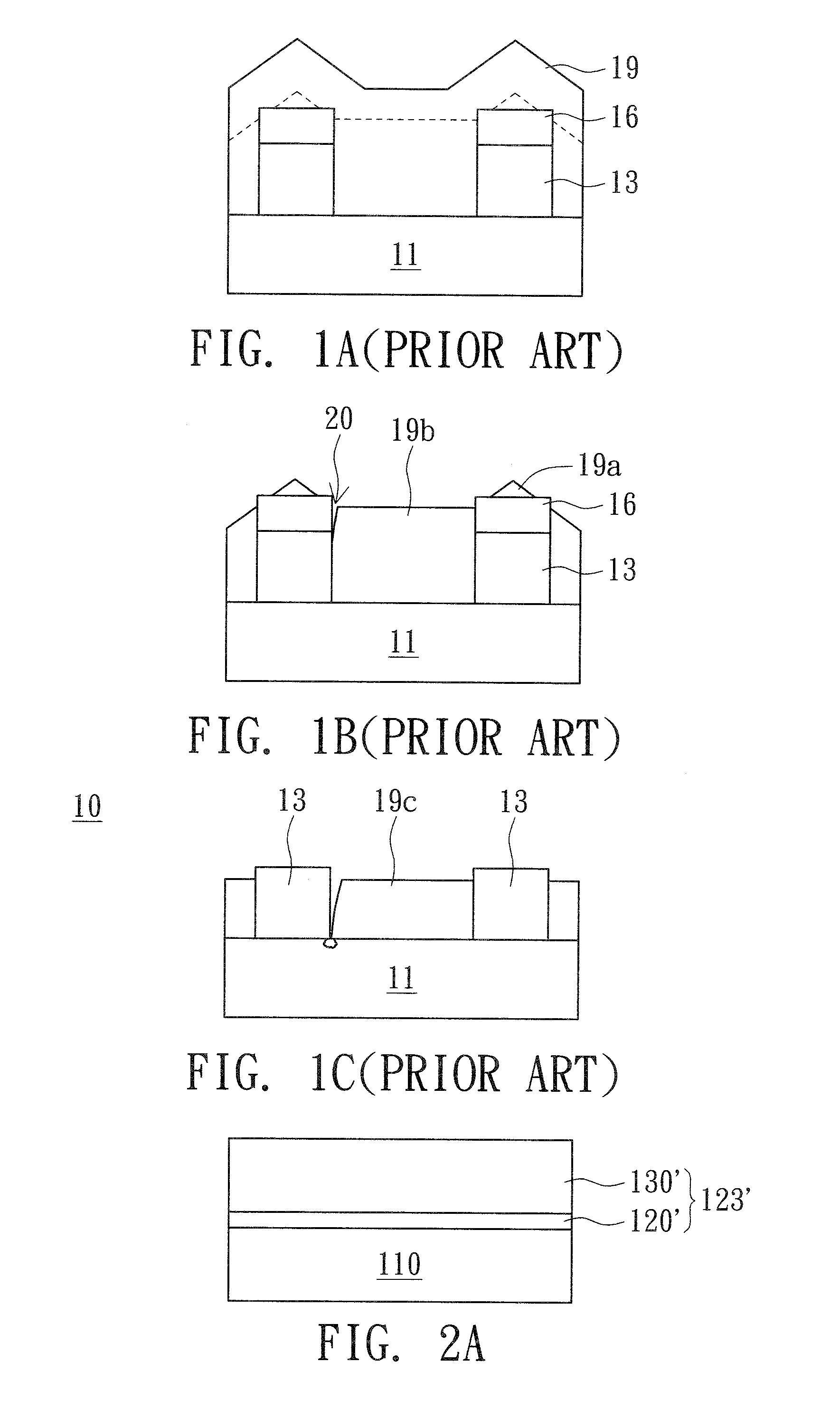
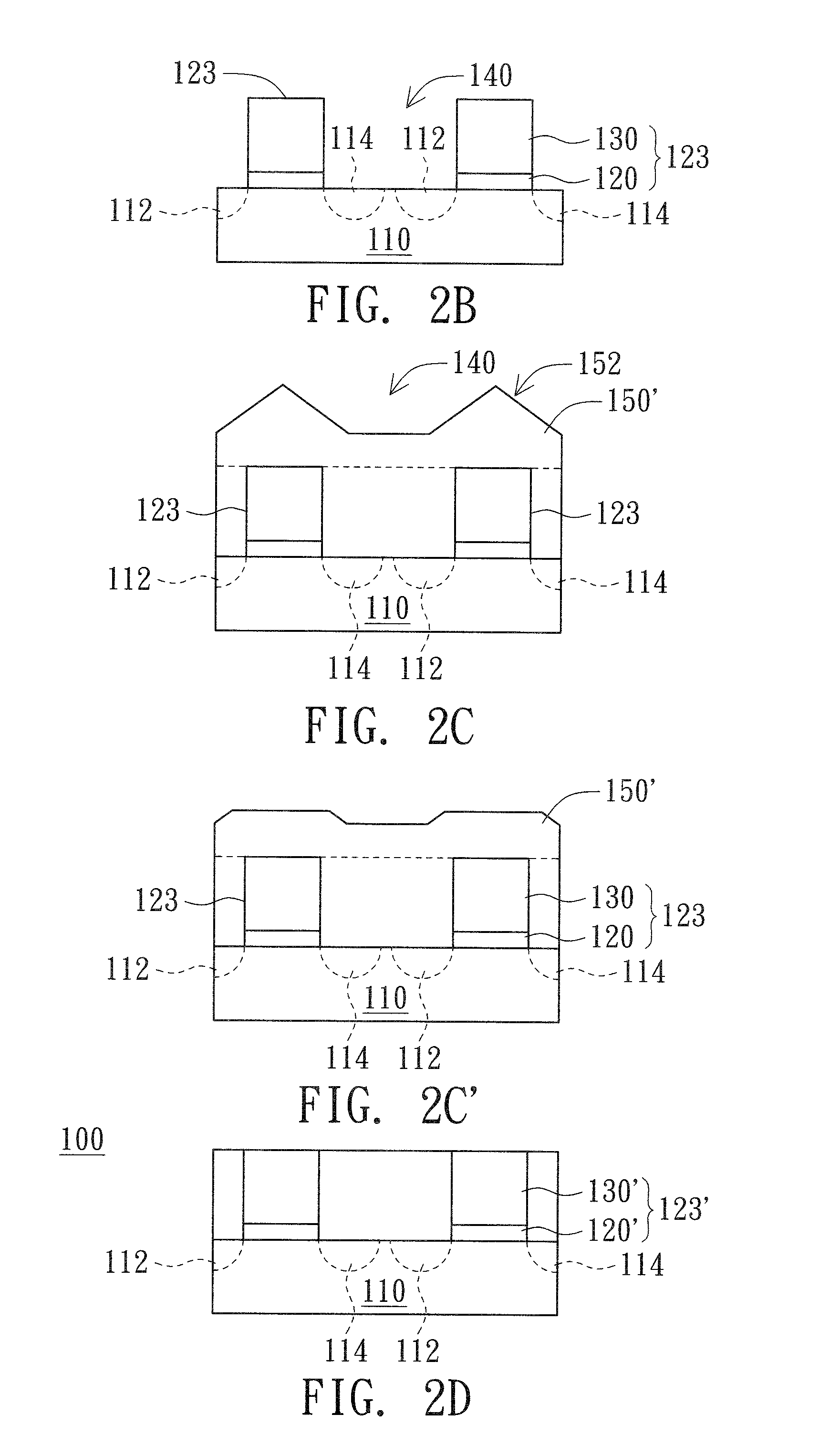
[0015]Referring to FIGS. 2A˜2D, cross-sectional view of diagrams illustrating a method of forming a non-volatile memory cell of the invention according to the first embodiment. The non-volatile memory for example, is read only memory (ROM), programmable read only memory (PROM), erasable programmable read only memory (EPROM), electrically erasable programmable read only memory (EEPROM), flash EEPROM, or nitride trap memory. The method of forming a non-volatile memory cell including following steps. Firstly, a substrate 110 is provided, and a stacking structure 123′ is then formed on the substrate, as shown in FIG. 2A. The stacking structure 123′ at least including an oxide-nitride-oxide (ONO) layer 120′ and a polysilicon layer 130′. The ONO layer 120′ is formed on the substrate 110, and the polysilicon layer 130′ is then formed on the ONO layer 120′. The ONO layer 120′ includes a top oxide layer, a nitride layer, and a bottom oxide layer. The top and the bottom oxide layer are thicke...

second embodiment

[0023]The method of the present embodiment differs from that of the first embodiment in the stopping layer on the top of the stacking structure during the polishing process. The same piece remains numerically labeled the same in the following drawings.

[0024]Referring to FIGS. 3A˜3D, cross sectional views illustrating a method of forming a non-volatile memory cell according to the second embodiment of the invention. Firstly, numerous stacking units 223 are formed on the substrate 110, as shown in FIG. 3A. Besides the ONO layer 120 and the polysilicon layer 130, the stacking units 223 further includes a stopping layer 235 formed on the polysilicon layer 130. Two implantation processes are then be performed to form the source region 112 and drain region 114. The stopping layer 235 is located on the top of the stacking units and blocks accelerating ions during the implantation, so that it prevents the polysilicon layer 130 from being doped. The stopping layer 235 also functions in the f...


PUM


Abstract

A method of forming a non-volatile memory cell is provided. The method comprises: (a) providing a substrate; (b) forming a stacking structure on the substrate, the stacking structure at least comprising an oxide-nitride-oxide layer (ONO layer) and a polysilicon layer thereon; (c) patterning the stacking structure to form a plurality of separated stacking units, each two stacking units having an aperture therebetween; (d) forming a source region and a drain region buried in the substrate at two sides of the each stacking unit; (e) forming an oxide layer in the aperture and over the stacking units; and (f) performing a chemical mechanical polishing (CMP) process to remove the oxide layer over the stacking units and outside the aperture.

Description

BACKGROUND OF THE INVENTION[0001]1. Field of the Invention[0002]The invention relates in general to a method of forming a non-volatile memory cell, and more particularly to a method of forming a non-volatile memory cell in combination with a chemical mechanical polishing process.[0003]2. Description of the Related Art[0004]The memory devices for non-volatile storage of information, such as read only memory (ROM), programmable read only memory (PROM), erasable programmable read only memory (EPROM), and other advanced memory devices, are currently used in the worldwide industries. The other advanced memory devices that involve more complex processing and testing procedures include electrically erasable programmable read only memory (EEPROM), and flash EEPROM. These advanced memory devices can accomplish the tasks that ROM can't do. For example, using EEPROM devices in circuitry permits in-circuit erasing and reprogramming of the device.[0005]The main characteristic of nitride trap mem...

Claims


Application Information

Patent Timeline
IPC IPC(8): H01L21/306
CPCH01L21/31053H01L27/11568H01L27/115H01L22/26H10B69/00H10B43/30
Inventor YEH, CHIN-TSANLO, CHIH-HSIENSU, CHIN-TACHEN, KUANG-CHAO
Owner MACRONIX INT CO LTD
Why Eureka
Try Eureka