A method for improving the breakdown voltage of gate oxide layer of trench vdmos device

A gate oxide layer and oxide layer technology, which is applied in semiconductor devices, semiconductor/solid-state device manufacturing, circuits, etc., can solve the problems of lower breakdown voltage, surface damage of epitaxial layer, and degradation of gate oxide layer quality, so as to improve the breakdown voltage. Breakthrough voltage, improvement of failure ratio, and quality assurance effect

Active Publication Date: 2017-08-25
FOUNDER MICROELECTRONICS INT
View PDF3 Cites 0 Cited by
  • Summary
  • Abstract
  • Description
  • Claims
  • Application Information

AI Technical Summary

Problems solved by technology

The above-mentioned operations are easy to cause damage to the surface of the epitaxial layer of the silicon substrate, resulting in a decrease in the quality of the gate oxide layer grown on the damaged site, a decrease in the breakdown voltage, and ultimately the failure of the device IGSS

Method used


Image

  • A method for improving the breakdown voltage of gate oxide layer of trench vdmos device
  • A method for improving the breakdown voltage of gate oxide layer of trench vdmos device
  • A method for improving the breakdown voltage of gate oxide layer of trench vdmos device

Examples


Embodiment 1

[0032] A method for improving the breakdown voltage of the gate oxide layer of the trench type VDMOS device of the present invention may comprise the steps of:

[0033] Step 1, providing a silicon substrate with an epitaxial layer;

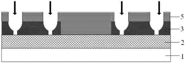
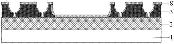
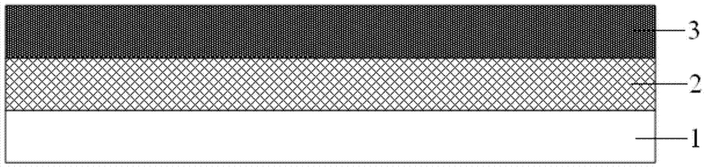
[0034] Specific as figure 1 As shown, the silicon substrate with an epitaxial layer can be a conventional epitaxial wafer in this field, and an epitaxial layer 2 can also be grown on a silicon substrate 1 by a conventional method in this field; An N-type epitaxial layer 2 is formed on one side surface of the silicon substrate 1 .

[0035] Step 2, forming an initial oxide layer on the epitaxial layer of the silicon substrate;

[0036] Specifically, the epitaxial layer 2 of the silicon substrate 1 can be formed by wet oxidation with a thickness of The initial oxide layer 3; in this embodiment, the thickness of the formed initial oxide layer 3 can be The temperature of wet oxidation may be 950°C.

[0037] Step 3, photolithography and etching, ...

Embodiment 2

[0055] Except step 10, the thickness of the gate oxide layer is Except, other is identical with embodiment 1. After testing, the breakdown voltage of the gate oxide layer of the trench VDMOS device in this embodiment is 94V.

Embodiment 3

[0057] Except step 10, the thickness of the gate oxide layer is Except, other is identical with embodiment 1. After testing, the breakdown voltage of the gate oxide layer of the trench VDMOS device in this embodiment is 50V.


PUM


Abstract

The invention provides a method for increasing breakdown voltage of a gate oxide layer of a groove-type VDMOS (Vertical Double-diffused Metal Oxide Semiconductor) device. The method comprises the following steps of providing a silicon substrate with an epitaxial layer, forming an initial oxide layer on the epitaxial layer of the silicon substrate, performing photoetching and etching, forming an active region graph on the initial oxide layer, performing ion injection, forming an active region in the epitaxial layer below the active region graph, performing the photoetching, forming a photoresist layer with a loop region graph and a gate graph, sequentially performing wet method etching and dry method etching, forming the loop region graph and the gate graph on the initial oxide layer, performing the ion injection, forming a loop region in the epitaxial layer below the loop region graph, removing the photoresist layer, forming a hard mask on the epitaxial layer and the initial oxide layer, performing the etching, forming a groove in the active region, removing the hard mask, and forming a gate above the gate graph. The method can effectively remove a damaged part on the surface of the epitaxial layer of the silicon substrate caused by operation such as the etching, so that the quality of the gate oxide layer of the device can be ensured.

Description

technical field [0001] The invention belongs to the technical field of semiconductor manufacturing, and in particular relates to a method for increasing the breakdown voltage of a gate oxide layer of a trench type VDMOS device. Background technique [0002] For trench VDMOS devices, the breakdown voltage of the gate oxide layer is a very important performance parameter. If the breakdown voltage of the gate oxide layer is low, it will lead to an increase in the failure ratio of gate-source leakage (IGSS), and even lead to the scrapping of the entire device in severe cases. [0003] In the manufacturing process of the initial ring region of the trench VDMOS device, operations such as ion implantation and etching are usually required, and the etching process includes wet etching and dry etching. Wet etching usually immerses the etching material in the etching solution for etching, which has good selectivity and isotropy, and the width of lateral etching is close to the depth o...

Claims


Application Information

Patent Timeline
Patent Type & Authority Patents(China)
IPC IPC(8): H01L21/336H01L21/316
CPCH01L29/42364H01L29/66712
Inventor 赵圣哲
Owner FOUNDER MICROELECTRONICS INT
Why Eureka
Try Eureka