Non-polar a-surface GaN-based ultraviolet photoelectric detector and preparation method thereof

An electric detector, non-polar technology, applied in the direction of circuits, electrical components, semiconductor devices, etc., can solve the problems of complex structure of ultraviolet photodetectors, hindering the performance of ultraviolet photodetectors, high time cost and process cost, etc., to achieve The effects of avoiding electric leakage, improving external quantum efficiency, and reducing lattice mismatch

Pending Publication Date: 2022-07-22
SOUTH CHINA UNIV OF TECH
View PDF0 Cites 0 Cited by
  • Summary
  • Abstract
  • Description
  • Claims
  • Application Information

AI Technical Summary

Problems solved by technology

[0003] However, most of the current commercial GaN-based ultraviolet photodetector materials use the c-plane ((0001) plane) as the epitaxial plane. This material has serious spontaneous polarization and piezoelectric polarization effects, resulting in strong built-in The electric field forms the Quantum-confined Starker Effect (QCSE), which separates the spatial distribution of electron and hole wave functions, causes energy band bending, reduces external quantum efficiency, and increases the dark current of the device. Unstable performance, which seriously hinders the improvement of the performance of UV photodetectors
In addition, the currently widely used p-n junction or p-i-n structure is restricted by two aspects. On the one hand, due to the unintentional doping of GaN itself, there is a high n-type background carrier concentration inside, and the Mg-doped Passivation in the GaN process prevents most of the Mg from being activated, resulting in difficulty in p-type doping, and it is difficult to prepare p-type materials with high hole concentration; The cost and process cost are relatively high, which is not conducive to mass production and manufacturing

Method used


Image

  • Non-polar a-surface GaN-based ultraviolet photoelectric detector and preparation method thereof
  • Non-polar a-surface GaN-based ultraviolet photoelectric detector and preparation method thereof
  • Non-polar a-surface GaN-based ultraviolet photoelectric detector and preparation method thereof

Examples


Embodiment 1

[0051] This embodiment provides a method for preparing a non-polar a-plane GaN-based ultraviolet photodetector, which specifically includes the following steps:

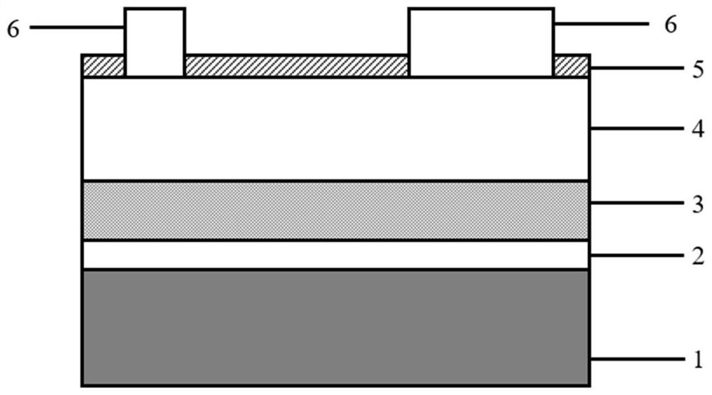
[0052] (1) If figure 1 As shown, an ultraviolet photodetector epitaxial wafer was grown on an r-plane sapphire substrate 1 by metal organic chemical vapor deposition technology, including a non-polar a-plane AlN buffer layer 2 and a non-polar a-plane Al with graded composition. x Ga 1-x The N buffer layer 3 and the non-polar a-plane GaN epitaxial layer 4, where x=0.2˜0.8.

[0053] (2) The surface of the ultraviolet photodetector epitaxial wafer obtained in step (1) is cleaned, soaked in acetone and anhydrous ethanol in sequence, and ultrasonically cleaned for 3 minutes, rinsed with deionized water after cleaning, and dried in hot high-purity nitrogen. .

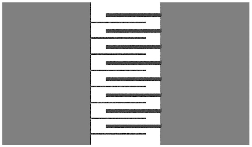
[0054] (3) Using plasma-assisted chemical vapor deposition to deposit a layer of Si on the surface of the ultraviolet photodetector epitaxial wafer obtained in s...

Embodiment 2

[0066] This embodiment provides a method for preparing a non-polar a-plane GaN asymmetric MSM type ultraviolet photodetector, which specifically includes:

[0067] (1) If figure 1 As shown, an ultraviolet photodetector epitaxial wafer was grown on an r-plane sapphire substrate 1 by metal organic chemical vapor deposition technology, including a non-polar a-plane AlN buffer layer 2 and a non-polar a-plane Al with graded composition. x Ga 1-x N buffer layer 3 and non-polar a-plane GaN epitaxial layer 4, wherein:

[0068] The non-polar a-plane AlN buffer layer 2 is grown on the r-plane sapphire substrate 1 with a thickness of 120 nm;

[0069] Compositionally graded nonpolar a-plane Al x Ga 1-x The N buffer layer 3 is grown on the non-polar a-plane AlN buffer layer 2 with a thickness of 450 nm;

[0070] Non-polar a-plane GaN epitaxial layers grown on compositionally graded non-polar a-plane Al x Ga 1-x On the N buffer layer 3, the thickness is 3 μm.

[0071] (2) The surfac...

Embodiment 3

[0082] This embodiment provides a method for preparing a non-polar a-plane GaN asymmetric MSM type ultraviolet photodetector, which specifically includes:

[0083] (1) If figure 1 As shown, an ultraviolet photodetector epitaxial wafer was grown on an r-plane sapphire substrate 1 by metal organic chemical vapor deposition technology, including a non-polar a-plane AlN buffer layer 2 and a non-polar a-plane Al with graded composition. x Ga 1-x N buffer layer 3 and non-polar a-plane GaN epitaxial layer 4, wherein:

[0084] The non-polar a-plane AlN buffer layer 2 is grown on the r-plane sapphire substrate with a thickness of 200 nm;

[0085] Compositionally graded nonpolar a-plane Al x Ga 1-x The N buffer layer 3 is grown on the non-polar a-plane AlN buffer layer 2 with a thickness of 600 nm;

[0086] Non-polar a-plane GaN epitaxial layers grown on compositionally graded non-polar a-plane Al x Ga 1-x On the N buffer layer 3, the thickness is 4 μm;

[0087] (2) The surface ...


PUM

PropertyMeasurementUnit
thicknessaaaaaaaaaa
thicknessaaaaaaaaaa
thicknessaaaaaaaaaa

Abstract

The invention discloses a non-polar a-surface GaN-based ultraviolet photoelectric detector and a preparation method thereof. The ultraviolet photoelectric detector comprises an ultraviolet photoelectric detector epitaxial wafer, a Si3N4 passivation layer deposited on the ultraviolet photoelectric detector epitaxial wafer, and a Schottky interdigital electrode of an asymmetric MSM structure. The ultraviolet photoelectric detector epitaxial wafer comprises a non-polar a-surface AlN buffer layer, a non-polar a-surface AlxGa1-xN buffer layer with gradually changed components and a non-polar a-surface GaN epitaxial layer which are sequentially grown on an r-surface sapphire substrate, wherein x is equal to 0.2-0.8; the Si3N4 passivation layer is arranged on the non-polar a-surface GaN epitaxial layer; and the Schottky interdigital electrode penetrates through the Si3N4 passivation layer and is in direct contact with the non-polar a-surface GaN epitaxial layer on the ultraviolet photoelectric detector epitaxial wafer. According to the invention, the high-performance non-polar a-surface GaN ultraviolet photoelectric detector is realized, the dark current of the device is reduced, and the stability is improved.

Description

technical field [0001] The invention relates to the technical field of ultraviolet photodetectors, in particular to a non-polar a-plane GaN-based ultraviolet photodetector and a preparation method thereof. Background technique [0002] Ultraviolet photodetectors are optoelectronic components that play an important role in missile guidance, space communication, environmental monitoring, and biochemical ultraviolet detection. The third-generation wide-bandgap semiconductor material, GaN, is very suitable for the production of high-frequency, high-power, high-integration electronic devices due to its large band gap, high electron mobility, good thermal stability, and strong radiation resistance. , which have been well used in the field of ultraviolet photodetectors. [0003] However, most commercial GaN-based UV photodetectors use the c-plane ((0001) plane) as the epitaxial plane. This material has serious spontaneous polarization and piezoelectric polarization effects, result...

Claims


Application Information

Patent Timeline
Patent Type & Authority Applications(China)
IPC IPC(8): H01L31/0224H01L31/102H01L31/18
CPCH01L31/022408H01L31/102H01L31/1852H01L31/1856
Inventor 王文樑张景鸿李国强李灏孔德麒
Owner SOUTH CHINA UNIV OF TECH
Why Eureka
Try Eureka