Fluorescent filtered electrophosphorescence

a technology of electrophosphorescence and fluorescence, which is applied in the direction of luminescnet screens, discharge tubes, organic semiconductor devices, etc., can solve the problems of limited operation stability and achieve the effects of stable color balance, enhanced stability, and increased drive voltag

Active Publication Date: 2010-08-03
UNIV OF SOUTHERN CALIFORNIA +1
View PDF19 Cites 33 Cited by
  • Summary
  • Abstract
  • Description
  • Claims
  • Application Information

AI Technical Summary

Benefits of technology

[0050]A key advantage of the present invention over the previous applications of electrophosphorescence is that separate colors can be emitted from the fluorescent and phosphorescent centers. For example, it a device according to an embodiment of the present invention may be constructed to have blue emission from a fluorescent dopant and green emission from the phosphorescent dopant. The result would be an OLED with an emission spectrum that was the sum of the blue and green emission spectra. Alternatively, a device according to another embodiment of the present invention may be used to prepare a white emissive OLED, in which the blue component of the spectrum is from the fluorescent dopant and the green-to-red (G-R) components of the white light are provided by the phosphorescent dopant(s). The G-R phosphor could be a single dopant that emits with a broad emission spectrum or two dopants, chosen such that the sum of their spectra cover the range from green to red. In this way, 25% of the excitons would produce blue light, while the remaining 75% are used for the G-R part of the emission spectrum. This is roughly the ratio of blue to G-R in the typical white OLED spectrum. This approach to a white OLED may have the benefit of a stable color balance as the drive voltage is increased and an enhanced stability. The enhanced stability results from having long lived fluorescent blue components coupled to long lived G-R phosphors in a single device.
[0051]Generally, an OLED comprises at least one organic layer disposed between and electrically connected to an anode and a cathode. When a current is applied, the anode injects holes and the cathode injects electrons into the organic layer(s). The injected holes and electrons each migrate toward the oppositely charged electrode. When an electron and hole localize on the same molecule, an “exciton,” which is a localized electron-hole pair having an excited energy state, is formed. Light is emitted when the exciton relaxes via a photoemissive mechanism. In some cases, the exciton may be localized on an excimer or an exciplex. Non-radiative mechanisms, such as thermal relaxation, may also occur, but are generally considered undesirable.
[0052]The initial OLEDs used emissive molecules that emitted light from their singlet states (“fluorescence”) as disclosed, for example, in U.S. Pat. No. 4,769,292, which is incorporated by reference in its entirety. Fluorescent emission generally occurs in a time frame of less than 10 nanoseconds.
[0053]More recently, OLEDs having emissive materials that emit light from triplet states (“phosphorescence”) have been demonstrated. Baldo et al., “Highly Efficient Phosphorescent Emission from Organic Electroluminescent Devices,” Nature, vol. 395, 151-154, 1998; (“Baldo-I”) and Baldo et al., “Very high-efficiency green organic light-emitting devices based on electrophosphorescence,” Appl. Phys. Lett., vol. 75, No. 3, 4-6 (1999) (“Baldo-II”), which are incorporated by reference in their entireties. Phosphorescence may be referred to as a “forbidden” transition because the transition requires a change in spin states, and quantum mechanics indicates that such a transition is not favored. As a result, phosphorescence generally occurs in a time frame exceeding at least 10 milliseconds, and typically greater than 100 milliseconds. If the natural radiative lifetime of phosphorescence is too long, triplets may decay by a non-radiative mechanism, such that no light is emitted. Organic phosphorescence is also often observed in molecules containing heteroatoms with unshared pairs of electrons at very low temperatures. 2,2′-Bipyridine is such a molecule. Non-radiative decay mechanisms are typically temperature dependent, such that an organic material that exhibits phosphorescence at liquid nitrogen temperatures typically does not exhibit phosphorescence at room temperature. But, as demonstrated by Baldo, this problem may be addressed by selecting phosphorescent compounds that do phosphoresce at room temperature. Representative emissive layers include doped or un-doped phosphorescent organometallic materials such as disclosed in U.S. Pat. Nos. 6,303,238 and 6,310,360; U.S. Patent Application Publication Nos. 2002-0034656; 2002-0182441; 2003-0072964; and WO-02 / 074015.
[0054]Generally, the excitons in an OLED are believed to be created in a ratio of about 3:1, i.e., approximately 75% triplets and 25% singlets. See, Adachi et al., “Nearly 100% Internal Phosphorescent Efficiency In An Organic Light Emitting Device,” J. Appl. Phys., 90, 5048 (2001), which is incorporated by reference in its entirety. In many cases, singlet excitons may readily transfer their energy to triplet excited states via “intersystem crossing,” whereas triplet excitons may not readily transfer their energy to singlet excited states. As a result, 100% internal quantum efficiency is theoretically possible with phosphorescent OLEDs. In a fluorescent device, the energy of triplet excitons is generally lost to radiationless decay processes that heat-up the device, resulting in much lower internal quantum efficiencies. OLEDs utilizing phosphorescent materials that emit from triplet excited states are disclosed, for example, in U.S. Pat. No. 6,303,238, which is incorporated by reference in its entirety.
[0055]Phosphorescence may be preceded by a transition from a triplet excited state to an intermediate non-triplet state from which the emissive decay occurs. For example, organic molecules coordinated to lanthanide elements often phosphoresce from excited states localized on the lanthanide metal. However, such materials do not phosphoresce directly from a triplet excited state but instead emit from an atomic excited state centered on the lanthanide metal ion. The europium diketonate complexes illustrate one group of these types of species.

Problems solved by technology

White OLEDs having only phosphorescent emissive materials may be highly efficient, but their operation stability is currently limited by the lifetime of the blue phosphorescent component.

Method used


Image

  • Fluorescent filtered electrophosphorescence
  • Fluorescent filtered electrophosphorescence
  • Fluorescent filtered electrophosphorescence

Examples


example 1

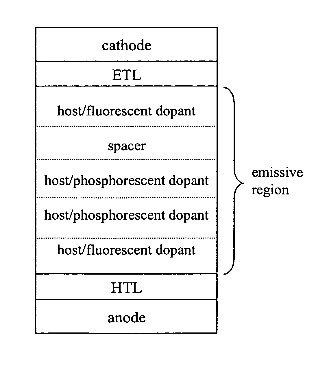
[0137]A device was prepared having the device structure:

ITO / NPD 300 Å / CBP:BCzVBi 5% 90 Å / CBP 40 Å / CBP:PQIr 3% 150 Å / CBP:Irppy 3% 50 Å / CBP 40 Å / CBP:BCzVBi 5%110 Å / BCP 320 Å / LiF 8 Å / Al 500 Å.

[0138]The principles discussed herein were used to make a WOLED with a maximum external quantum efficiency (ηext) of 9.2% at 1.8 mA / cm2, which is comparable to or higher than reported WOLEDs using all phosphorescent dopants. The excitation voltage of the whole device may be approximately 20% less than the corresponding WOLEDs using a blue phosphorescent dopant and thus the peak total power efficiency is improved to 19.2 lm / W. Blue emission versus green-and-red emission is in the ratio close to the ideal ratio of singlet (25%) to triplet (75%). The resulting highly balanced white light gives a color rendering index of 85. By making the phosphorescent doping layers away from the exciton generation region which has highly concentrated local triplet density, the triplet-triplet annihilation is red...

example 2

[0143]Devices were prepared having the following structures for the emissive region:[0144]I: NPD 300 Å / CBP:BCzVBi (5%, 50 Å) / CBP (160 Å) / CBP:BCzVBi (5%, 50 Å) / BCP 400 Å[0145]II: NPD 300 Å / CBP:BCzVBi (5%, 250 Å) / BCP 400 Å[0146]III: NPD 300 Å / CBP:BCzVBi (5%, 50 Å) / CBP (50 Å) / CBP:Ir(ppy)3 (2%, 150 Å) / CBP (50 Å) / CBP:BCzVBi (5%, 50 Å) / BCP 400 Å

[0147]Maximum quantum efficiencies of 2.6%, 2.7%, and 5.2% were measured for device I, II, and III, respectively.

[0148]FIG. 10 shown the emission spectrum of the devices I, II, and III at a current densities of 100 mA / cm2. Comparison of the non-normalized electroluminescence (EL) intensity for these three devices shows that insertion of an extra fluorescent layer in the middle of the emissive region does not give extra fluorescent emission. This confirms that the excitons are mainly generated at NPD / CBP and CBP / BCP interfaces, where charge carriers accumulate. Together with the fact that no CBP emission at short wavelength is observable in either d...

example 3

[0149]Devices were prepared having the following structures for the emissive region: NPD (300 Å) / CBP (x Å) / CBP:Ir(ppy)3 (5%, 50 Å) / CBP ((2000−x) Å) / BCP (330 Å) with x=0, 500, 1000, 1500 and 2000 Å for device I, II, III, IV, and V respectively.

[0150]The trend of ηext vs. position x indicates local triplet density is much higher at HTL / EML and EML / ETL interfaces than in the middle region of CBP emission layer, which agrees with the previous discussion about exciton formation zone and triplet diffusion. The comparison of the roll-off effect due to triplet-triplet annihilation by plotting the decreasing slope of ηext per decade of current density for these five devices shows that the roll-off effect is much stronger when the phosphorescent-doped region is adjacent to the exciton generation zone than when the phosphorescent-doped region is 500 Å away from it. This agrees with the reduced roll-off effect of ηext observed in the devices of the invention compared with other reported WOLEDs ...


PUM

PropertyMeasurementUnit
CRIaaaaaaaaaa
CRIaaaaaaaaaa
CRIaaaaaaaaaa

Abstract

The present invention relates to organic light emitting devices (OLEDs), and more specifically to OLEDS that emit light using a combination of fluorescent emitters and phosphorescent emitters for the efficient utilization of all of the electrically generated excitons.

Description

RELATED APPLICATIONS[0001]This application is a continuation-in-part of U.S. application Ser. No. 11 / 143,319, filed Jun. 1, 2005 now U.S. Pat. No. 7,474,048, and also claims the benefit of U.S. Provisional Patent Application No.: 60 / 738,252, filed Nov. 18, 2005; U.S. Provisional Patent Application No.: 60 / 738,868, filed Nov. 22, 2005; and U.S. Provisional Patent Application No.: 60 / 781,676, filed Mar. 13, 2006, which are incorporated herein by reference in their entirety.GOVERNMENT RIGHTS[0002]This invention was made with Government support under Contract No. DE-FC26-04NT42272 awarded by the Department of Energy. The government has certain rights in this invention.RESEARCH AGREEMENTS[0003]The claimed invention was made by, on behalf of, and / or in connection with one or more of the following parties to a joint university corporation research agreement: Princeton University, The University of Southern California, and the Universal Display Corporation. The agreement was in effect on an...

Claims


Application Information

Patent Timeline
Patent Type & Authority Patents(United States)
IPC IPC(8): H05B33/00
CPCH01L51/0072H01L51/0085H01L51/50H01L51/5016H01L51/5096H01L51/504H01L51/5044H01L2251/308H01L2251/5376H10K85/6572H10K85/342H10K50/131H10K50/13H10K50/11H10K2101/10H10K50/18H10K50/00H10K2102/103H10K2101/27
Inventor FORREST, STEPHENSUN, YIRUGIEBINK, NOELTHOMPSON, MARK E.
Owner UNIV OF SOUTHERN CALIFORNIA
Why Eureka
Try Eureka