Compact lens turret assembly

a technology of optical turrets and compact lenses, which is applied in the direction of radio frequency controlled devices, instruments, television systems, etc., can solve the problems of complicated assembly design, increased overall device size, and difficulty in precise positioning

Active Publication Date: 2010-08-03
TESSERA INC
View PDF33 Cites 95 Cited by
  • Summary
  • Abstract
  • Description
  • Claims
  • Application Information

AI Technical Summary

Problems solved by technology

This increases the size of the overall device.
This problem is particularly acute in the case of very compact devices as, for example, cameras incorporated in cellular telephones and personal digital assistants (“PDAs”).
The need for such precise positioning complicates the design of the assembly and, in some cases, may further aggravate the turret size problem noted above.
However, image-sensing chips are susceptible to mechanical damage and to chemical attack by atmospheric contaminants.
Moreover, bare imaging sensing chips are extremely sensitive to particulate contamination.
Moreover, such processes often suffer from high defect rates caused by particulate contamination.
Both of these factors tend to increase the cost of the resulting assemblies.
Moreover, these assemblies as well typically require turrets having areas substantially larger than the area of the chip itself.

Method used


Image

  • Compact lens turret assembly
  • Compact lens turret assembly
  • Compact lens turret assembly

Examples


Embodiment Construction

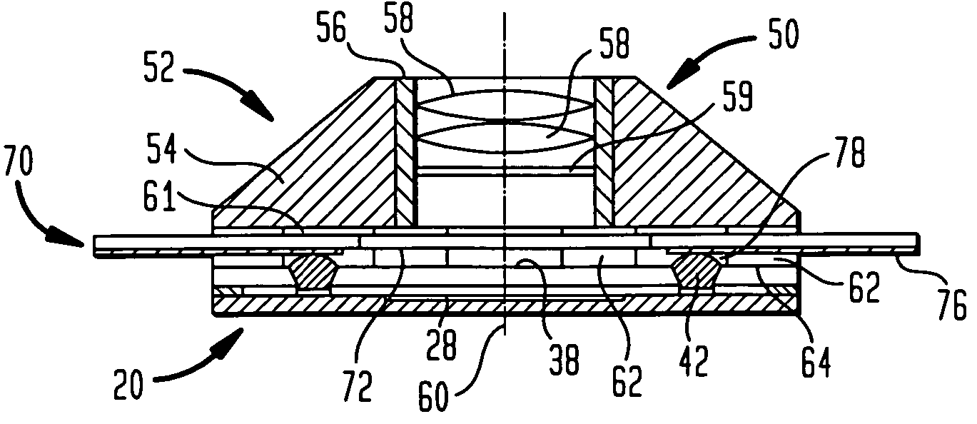
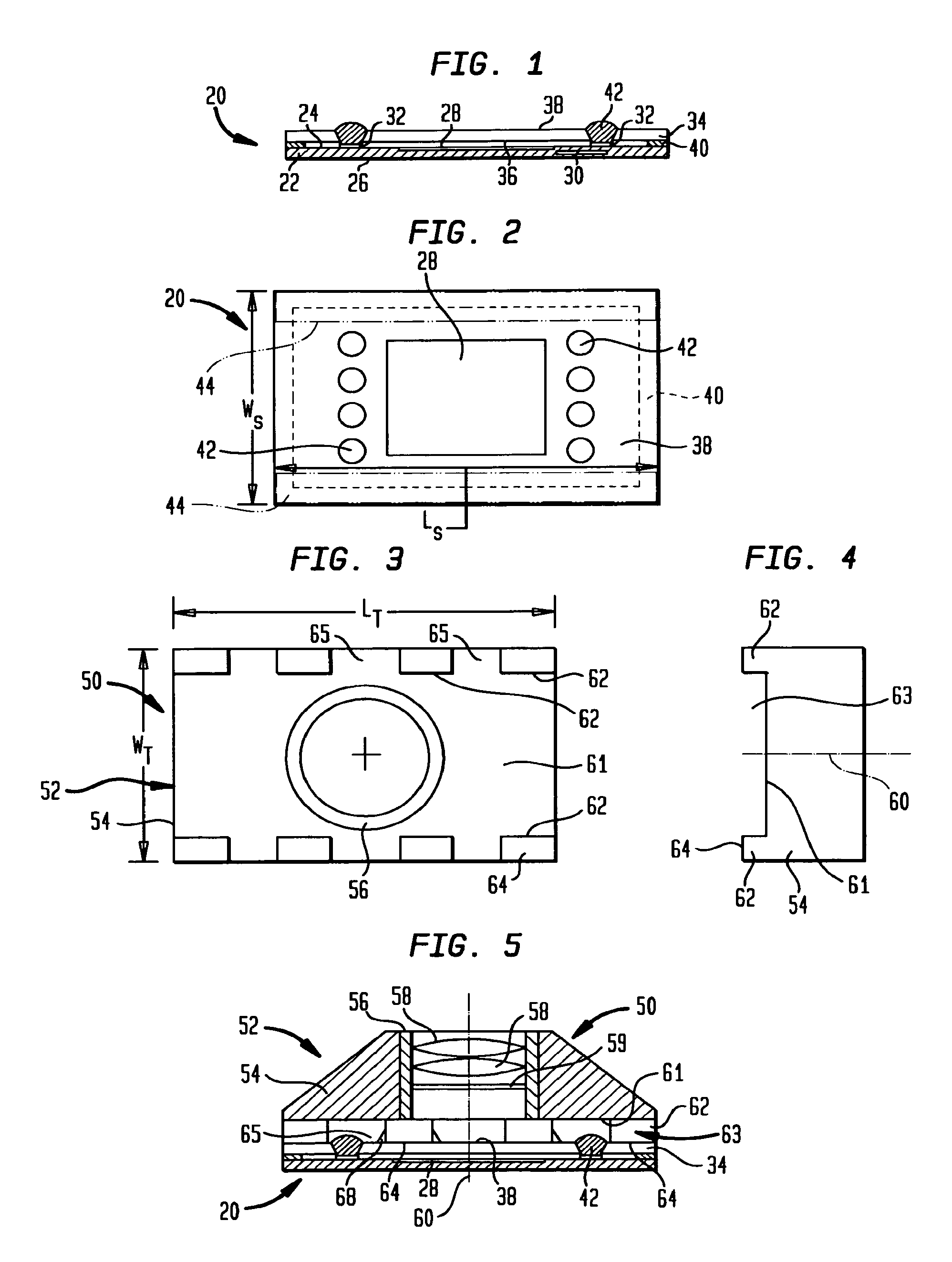
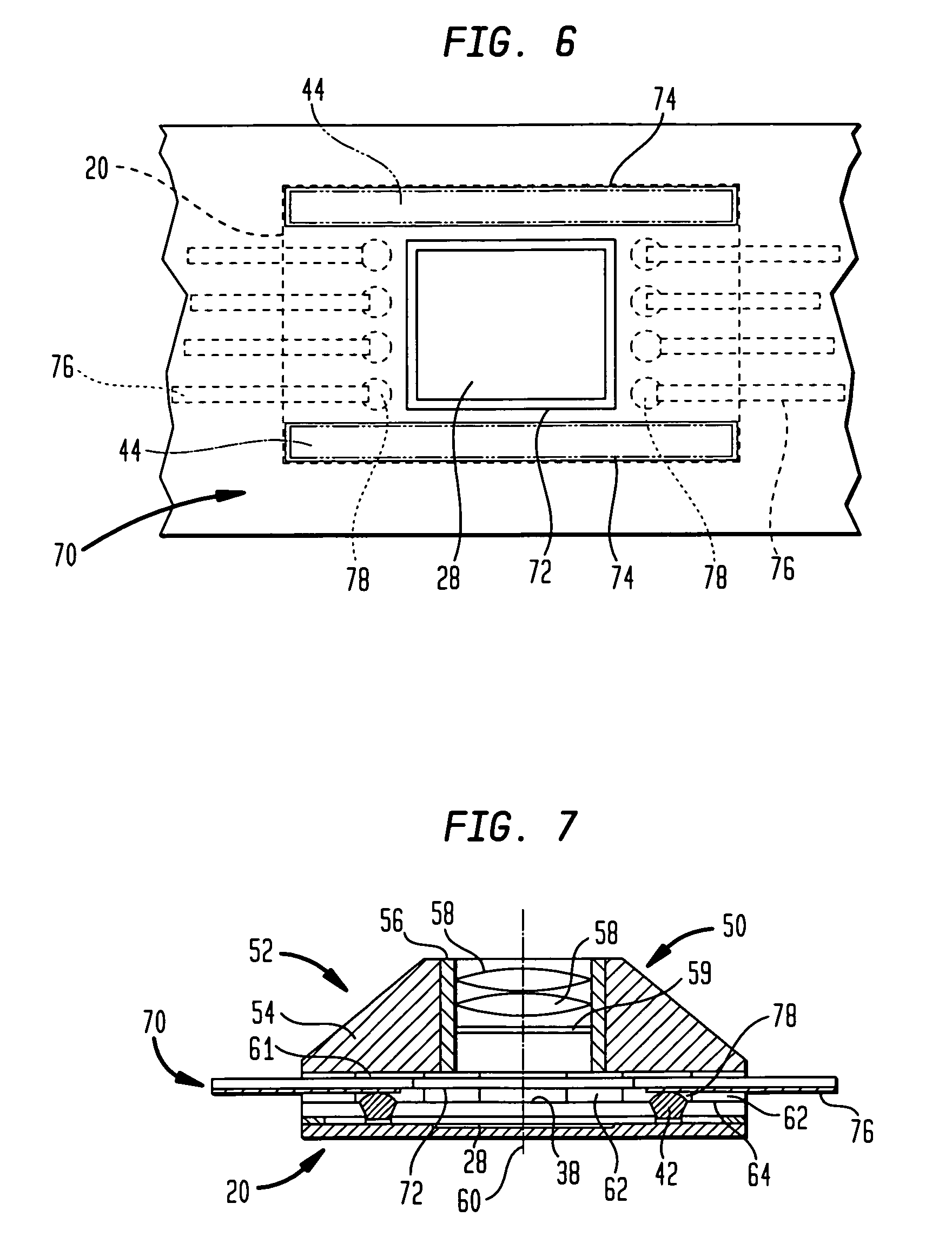
[0024]A module in accordance with one embodiment of the present invention includes a sensor unit 20 (FIGS. 1 and 2). Sensor unit 20 includes a semiconductor chip 22 having a front or top surface 24 and an oppositely directed rear or bottom surface 26. Front surface 24 includes an imaging area 28. Chip 22 includes electronic circuits, schematically indicated at 30 in FIG. 1, for generating one or more electrical signals representing an optical image impinging on imaging area 28. Numerous electrical circuits are well known in the imaging art for this purpose. For example, the semiconductor chip 22 may be a generally conventional charge-coupled device (CCD) imaging chip with conventional circuits such as clocking and charge-to-voltage conversion circuits. Any other conventional circuits may be used. Chip 22 has electrical connections or contacts 32 exposed at front surface 24 and electrically connected to the internal circuitry 30.

[0025]Sensor unit 20 also includes a cover 34 having an...


PUM


Abstract

An electronic camera module incorporates a sensor unit (20) having a semiconductor chip (22) such as a CCD imager and a cover (34) overlying the front surface of the chip. An optical unit (50) includes one or more optical elements such as lenses (58). The optical unit has engagement features (64) which abut alignment features on the sensor unit as, for example, portions (44) of the cover outer surface (38), so as to maintain a precise relationship between the optical unit and sensor unit.

Description

CROSS-REFERENCE TO RELATED APPLICATIONS[0001]The present application claims the benefit of the filing date of U.S. Provisional Patent Application No. 60 / 568,052, filed May 4, 2004, the disclosure of which is hereby incorporated herein by reference.FIELD OF THE INVENTION[0002]The present invention relates to the mounting and packaging of opto-electronic devices such as solid-state image sensors.BACKGROUND OF THE INVENTION[0003]Numerous electronic devices such as common electronic still cameras and video cameras include solid-state image sensors. A typical solid-state image sensor is formed in a semiconductor chip and includes an array of light-sensitive elements disposed in an area of the front surface of the chip, referred to herein as the “imaging area.” A color-sensitive image-sensing chip may include arrays of elements sensitive to different wavelengths of light. Each light-sensitive element is arranged to generate an electrical signal representing light falling on a particular s...

Claims


Application Information

Patent Timeline
Patent Type & Authority Patents(United States)
IPC IPC(8): H04N5/225G02B7/02H01L27/146H01L31/0203H01L31/0232
CPCG02B7/02H01L27/14618H01L27/14625H01L31/0203H01L31/0232H04N5/2253H04N5/2254H01L2924/0002H01L31/02325H04N23/54H01L2924/00
Inventor HUMPSTON, GILES
Owner TESSERA INC
Why Eureka
Try Eureka