Thermoelectric device with thin film elements, apparatus and stacks having the same

a technology of thin film elements and thermoelectric devices, which is applied in the direction of lighting and heating apparatus, machines using electric/magnetic effects, refrigerating machines, etc., can solve the problems of inefficient thermoelectric power conversion of this conventional thermoelectric apparatus, poor performance of a conventional device having thermoelectric thin films constructed based on a typical semiconductor, etc., and achieve the effect of improving the efficiency of the thermoelectric device constructed according to the embodiments of the present invention

Inactive Publication Date: 2010-08-17
IND TECH RES INST
View PDF14 Cites 17 Cited by
  • Summary
  • Abstract
  • Description
  • Claims
  • Application Information

AI Technical Summary

Benefits of technology

[0010]It is therefore an object of the present invention to provide a thermoelectric device with thin film elements, apparatus and stacks having the same. The structure designed according to the present invention has sufficient distance between the hot side and the cold side of the thermoelectric device, and the conventional heat-reflux problem (resulted from the extremely small distance between the hot side and the cold side) can be avoided. Thus, the efficiency of the thermoelectric device constructed according to the embodiments of the present invention can be effectively improved by using high ZT thermoelectric materials without a waste.

Problems solved by technology

However, the thermoelectric power conversion of this conventional thermoelectric apparatus is inefficient due to the limitation of bulky thermoelectric material property with low Figure of Merit (ZT) value.
Many experiments studying thermoelectric materials and researches attempting to improve performance of thermoelectric devices have been underway for the past 20-30 years with not much success.
However, the performance of a conventional device having thermoelectric thin films constructed based on a typical semiconductor is not very well. FIG. 2 is a cross-sectional view of a conventional device having thermoelectric thin films.
Although it have been proved that the thermoelectric thin films have high ZT value, the performance of the thermoelectric device is not as good as expected if the thermoelectric thin films are directly adopted into the conventional structure of device.
On the other words, it is not sufficient to sustain the temperature difference between the hot side and the cold side of the thermoelectric device in a meaningful time.
Moreover, factors that affect the electrical resistance and heat transmission resistance of the interface between the metal layers and the thermoelectric thin films have become considerable.
Joule's heating also affects the efficiency of thermoelectric device.
Therefore, the performances of conventional thermoelectric structure inside which the thermoelectric thin films have been inserted are not as great as expected.

Method used


Image

  • Thermoelectric device with thin film elements, apparatus and stacks having the same
  • Thermoelectric device with thin film elements, apparatus and stacks having the same
  • Thermoelectric device with thin film elements, apparatus and stacks having the same

Examples


first embodiment

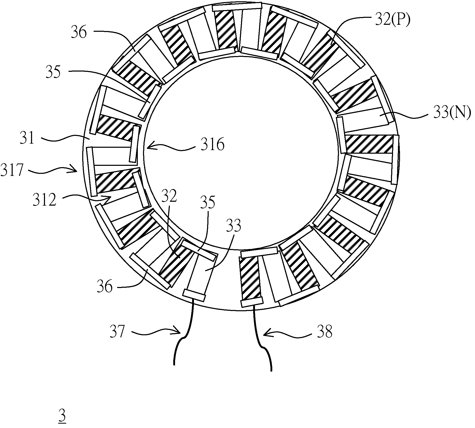
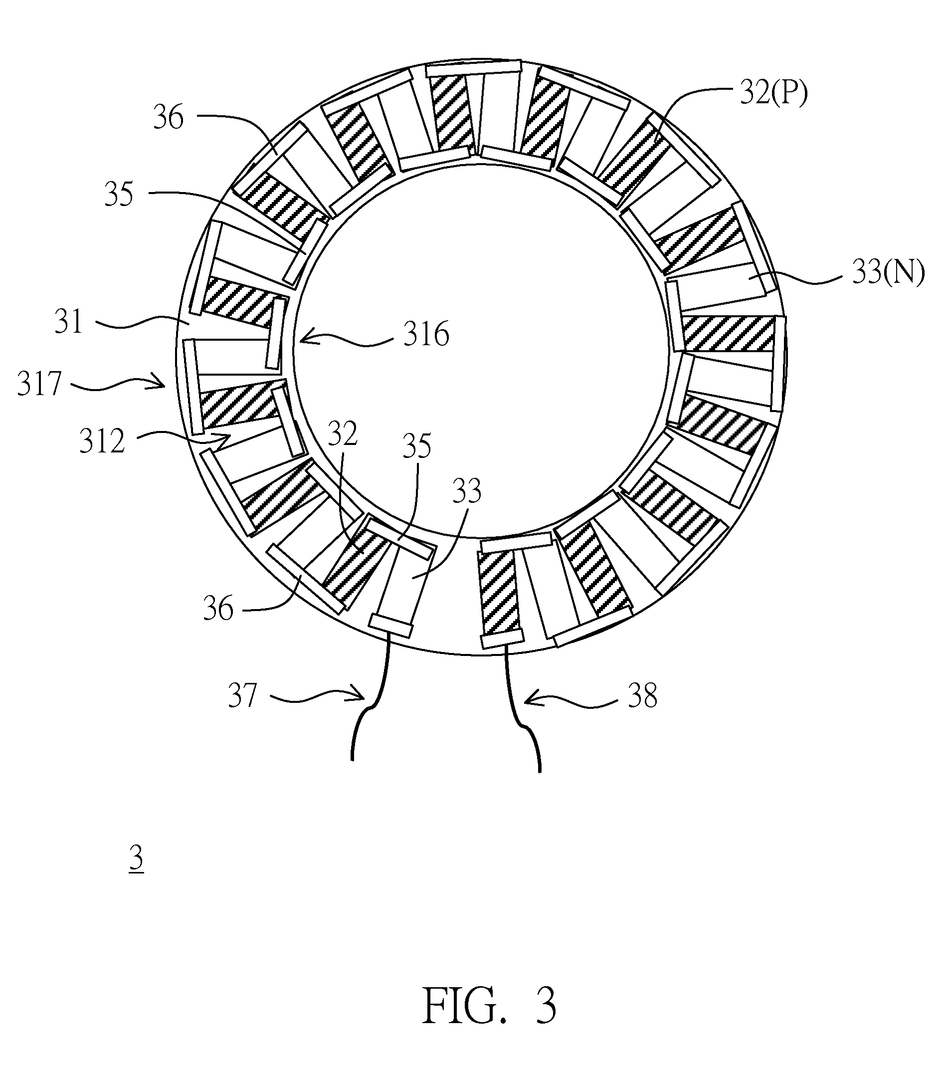
[0026]FIG. 3 is a top view of a thermoelectric device with thin film elements according to the first embodiment of the present invention. The thermoelectric device 3 includes a ring-shaped insulated substrate 31 and plural sets of thermoelectric thin film material pair (TEP) disposed thereon. The ring-shaped insulated substrate 31 has a first surface 312, an inner rim 316 and an outer rim 317. Those sets of TEP electrically connected to each other are disposed on the first surface 312 of the ring-shaped insulated substrate 31. Each set of TEP includes a P-type thermoelectric thin film element (TEE) 32 and an N-type thermoelectric thin film element (TEE) 33 electrically connected to each other. Also, the N-type TEE 33 of each set of TEP is electrically connected to the P-type TEE 32 of the adjacent set of TEP. Each of the P-type TEE 32 and the N-type TEE 33 has a thickness in a range of 10 nm to 200 μm. Additionally, the sets of thermoelectric thin film material pair (TEP) are electr...

second embodiment

[0036]In the second embodiment, a thermoelectric apparatus is disclosed, which is constructed by attaching insulation layers to upper side and lower side of the thermoelectric device of the first embodiment. In the practical applications of the conversion power of cooling / heating or electricity generation, the thermoelectric apparatus could be assembled with a heat conduction module. In the second embodiment, the front and rear surfaces of the substrate includes several sets of thermoelectric thin film material pair (TEP).

[0037]FIG. 5A and FIG. 5B are cross-sectional view of a thermoelectric apparatus having thermoelectric device with thin film elements according to the second embodiment of the present invention, wherein FIG. 5B illustrates the apparatus of FIG. 5A after assembly. The components in FIG. 5A and FIG. 5B identical to that in FIG. 4B are denoted with the same reference numbers.

[0038]As shown in FIG. 5A, a thermoelectric device with thin film elements 4, including a ring...

third embodiment

[0048]In the first and second embodiments, only one ring-shaped insulated substrate 31 is used in the thermoelectric device. In the practical applications, however, two or more ring-shaped insulated substrates could be laminated to form a stack of thermoelectric devices for enhancing the efficiency of thermoelectric conversion. It is, of course, noted that plural sets of TEP could be formed on either one surface or both (i.e. front and rear) surfaces of each substrate, and the present invention has no limitation herein.

[0049]FIG. 8A and FIG. 8B are cross-sectional view of a stack of thermoelectric devices with thin film elements according to the third embodiment of the present invention, wherein FIG. 8B illustrates the stack of FIG. 8A after assembly. Also, the stack constructed by two ring-shaped insulated substrates is illustrated in the third embodiment.

[0050]In the third embodiment, the stack 8 includes a first insulation layer 81, a first thermoelectric device 4a, a second insu...


PUM


Abstract

A thermoelectric device at least includes a ring-shaped insulated substrate and plural sets of thermoelectric thin film material pair (TEP) disposed thereon. The ring-shaped insulated substrate has an inner rim, an outer rim and a first surface. The sets of TEP electrically connected to each other are disposed on the first surface of the ring-shaped insulated substrate. Each set of TEP includes a P-type and an N-type thermoelectric thin film elements (TEE) electrically connected to each other. Also, the N-type TEE of each set is electrically connected to the P-type TEE of the adjacent set of TEP. When a current flows through the sets of TEP along a direction parallel to the surfaces of P-type and N-type thermoelectric thin film elements, a temperature difference is generated between the inner rim and the outer rim of the ring-shaped insulated substrate.

Description

[0001]This application claims the benefit of Taiwan application Serial No. 96150972, filed Dec. 28, 2008, the subject matter of which is incorporated herein by reference.BACKGROUND OF THE INVENTION[0002]1. Field of the Invention[0003]The invention relates in general to a thermoelectric device with thin film elements and stacks having the same, and more particularly to the thermoelectric device with thin film elements and stacks having the same with highly thermoelectric efficiency of power conversion for cooling / heating and electricity generation.[0004]2. Description of the Related Art[0005]A thermoelectric device is a module with properties of direct conversion of temperature differences to electric voltage and vice versa. Due to this property of thermoelectric conversion, both cooling / heating and power conversion applications are possible with emerging thermoelectric technologies. For example, this thermoelectric effect can be used to generate electricity, to measure temperature, ...

Claims


Application Information

Patent Timeline
Patent Type & Authority Patents(United States)
IPC IPC(8): H01L35/28
CPCH01L35/32H10N10/17
Inventor CHU, HSU-SHEN
Owner IND TECH RES INST
Why Eureka
Try Eureka