

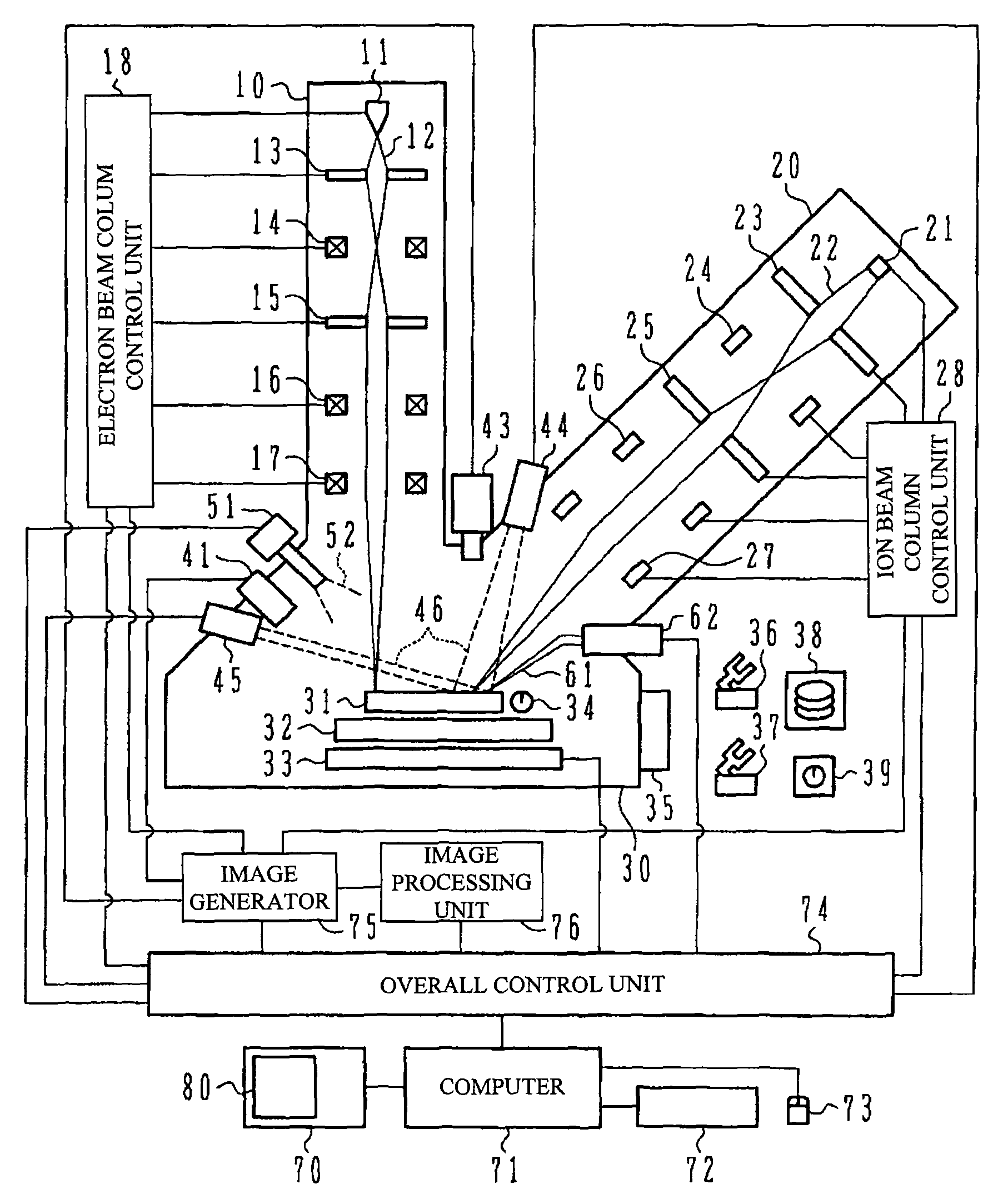
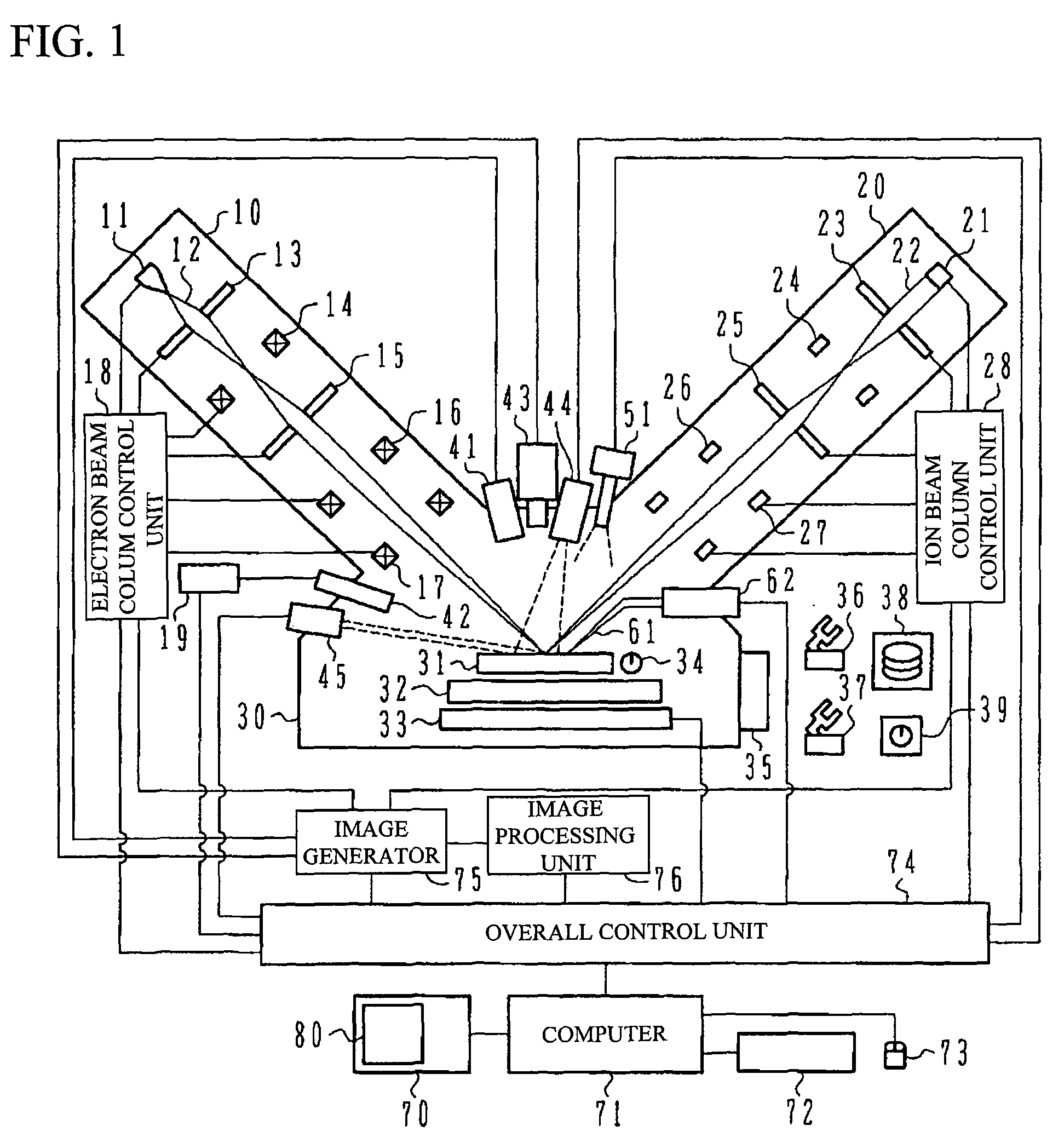
Charge particle beam system, sample processing method, and semiconductor inspection system
a particle beam and sample processing technology, applied in material analysis using wave/particle radiation, instruments, nuclear engineering, etc., can solve problems such as yield drop
- Summary
- Abstract
- Description
- Claims
- Application Information
AI Technical Summary
Benefits of technology
Problems solved by technology
Method used
Image

Examples
example 1
[0068]FIG. 4 shows a flowchart of a first example of the procedure for analyzing (reviewing) a defect portion of a sample detected by a separate optical inspection system, using the semiconductor inspection system of the present embodiment.
[0069]In the following, the defect analysis procedure using the semiconductor inspection system of the present embodiment is described with reference to FIG. 4.
[0070]When the semiconductor inspection system of the present embodiment is used for the wafer defect inspection in a semiconductor device manufacturing process, the sample (wafer) 31 is loaded in step S101. Prior to loading, the sample 31 that has been subjected to defect inspection by the separate optical inspection system is stored in the sample case 38 in advance and mounted on the load port.
[0071]Upon instruction from the computer 71 to start inspection with the sample 31 stored in the sample case 38, the overall control unit 74 outputs an instruction signal to the sample transfer robo...
example 2
[0092]FIG. 17 shows a flowchart of a second example of the procedure for analyzing (reviewing) the defect portion of a sample detected by a separate optical inspection system, using the semiconductor inspection system of the present embodiment.
[0093]The present example represents a process flow suitable for an accurate analysis of the particle 65 that exists in the film and that cannot be sufficiently observed by the SEM image by the scan of the electron beam 12 or by the SIM image by the scan of the ion beam 22, using a microscope image at higher resolution.
[0094]In the present example, the sample 31 and the cartridge 34 are mounted on the sample holder 32 in step S201, as described with reference to FIGS. 5 and 6, and then the sample holder is delivered into the sample chamber 30.
[0095]S202, S203, and S204 are the same as S102, 103, and 104 of FIG. 4. The defective site of the sample 31 delivered in the sample chamber 30 is detected by the optical microscope 43. If the defect dete...
example 3
[0105]FIG. 25 shows a flowchart of a third example of the procedure for analyzing (reviewing) the defect portion of the sample detected by the separate optical inspection system, using the semiconductor inspection system of the present embodiment
[0106]The present example also involves a method of analysis suitable for the accurate analysis of a particle that exists in the film and that cannot be observed with an SEM image or SIM image sufficiently, using an electron microscope image with higher resolution. The third example is characterized by the manner of use of the probe 61, in comparison with the second example.
[0107]S301 to S304 are the same as S101 to S104 of the first example. If the detection of a defective site by the optical microscopic image is successful and the determination in S303 is satisfied, the procedure moves to S305.
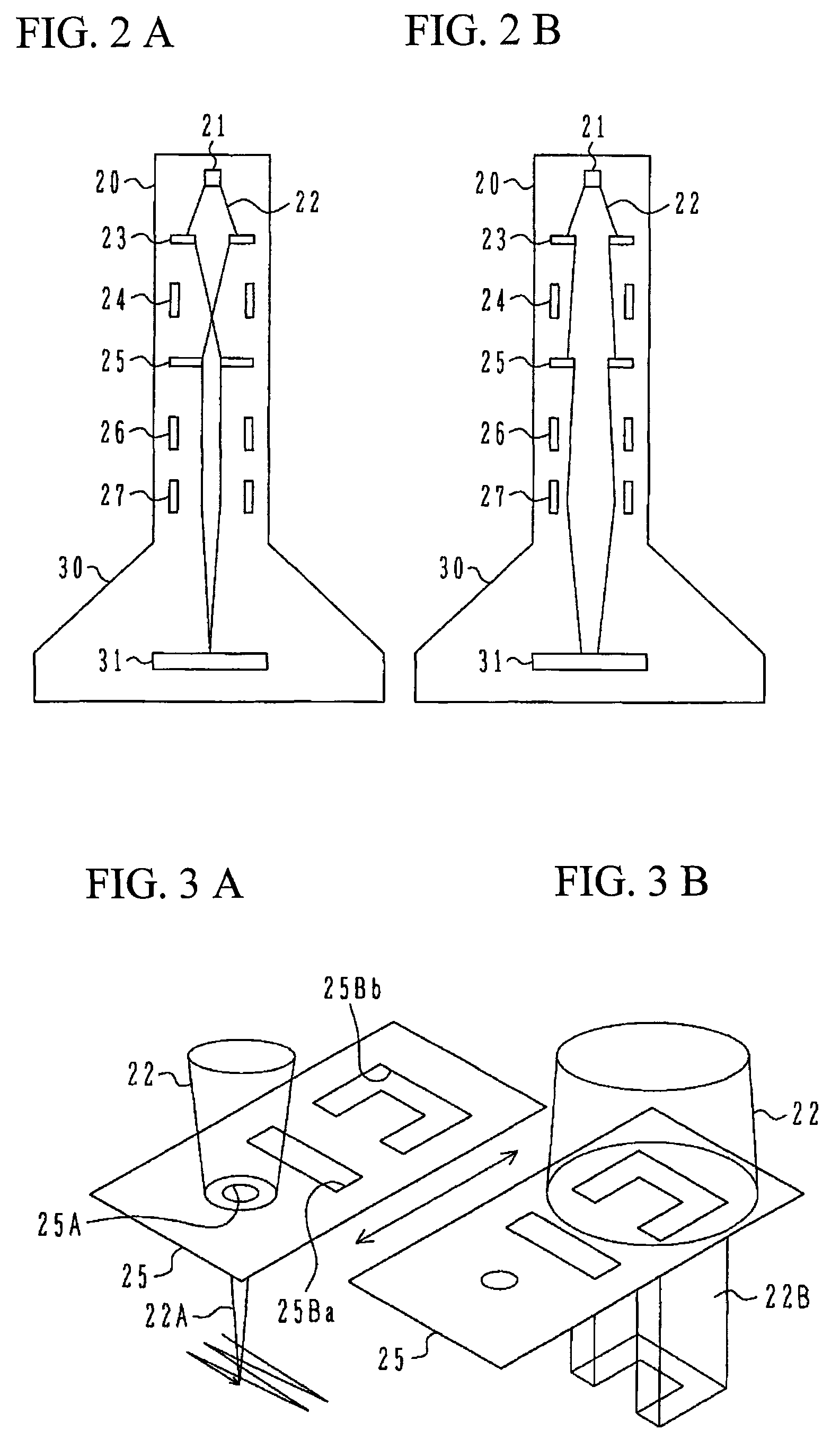
[0108]FIG. 26 shows a structure for the detection of the particle 65 that exists in the film using the dark field light source 44 and the optical mi...
PUM
| Property | Measurement | Unit |
|---|---|---|
| microscope | aaaaa | aaaaa |
| electron microscope | aaaaa | aaaaa |
| ion microscope | aaaaa | aaaaa |
Abstract
Description
Claims
Application Information