Techniques for forming shallow junctions

a technology of shallow junctions and junctions, which is applied in the direction of irradiation devices, electric discharge tubes, electrical apparatus, etc., can solve the problems of more end-of-range defects, diffusion-less anneal alone may not be enough to prevent all the ion-implanted dopants

Active Publication Date: 2008-05-08
VARIAN SEMICON EQUIP ASSOC INC
View PDF19 Cites 128 Cited by
  • Summary
  • Abstract
  • Description
  • Claims
  • Application Information

AI Technical Summary

Benefits of technology

[0010]Techniques for forming shallow junctions are disclosed. In one particular exemplary embodiment, the techniques may be realized as a method for forming shallow junctions. The method may comprise generating an ion beam comprising molecular ions based on one or more materials selected from a group consisting of: digermane (Ge2H6...

Problems solved by technology

As a result, a thinner amorphous layer may lead to a deeper junction depth, a less abrupt doping profile, an inadequate activation of dopants, and more end-of-range defects after anneal, all of which represent major obstacles in modern CMOS device miniaturization, especially for source-drain exte...

Method used


Image

  • Techniques for forming shallow junctions
  • Techniques for forming shallow junctions
  • Techniques for forming shallow junctions

Examples


Embodiment Construction

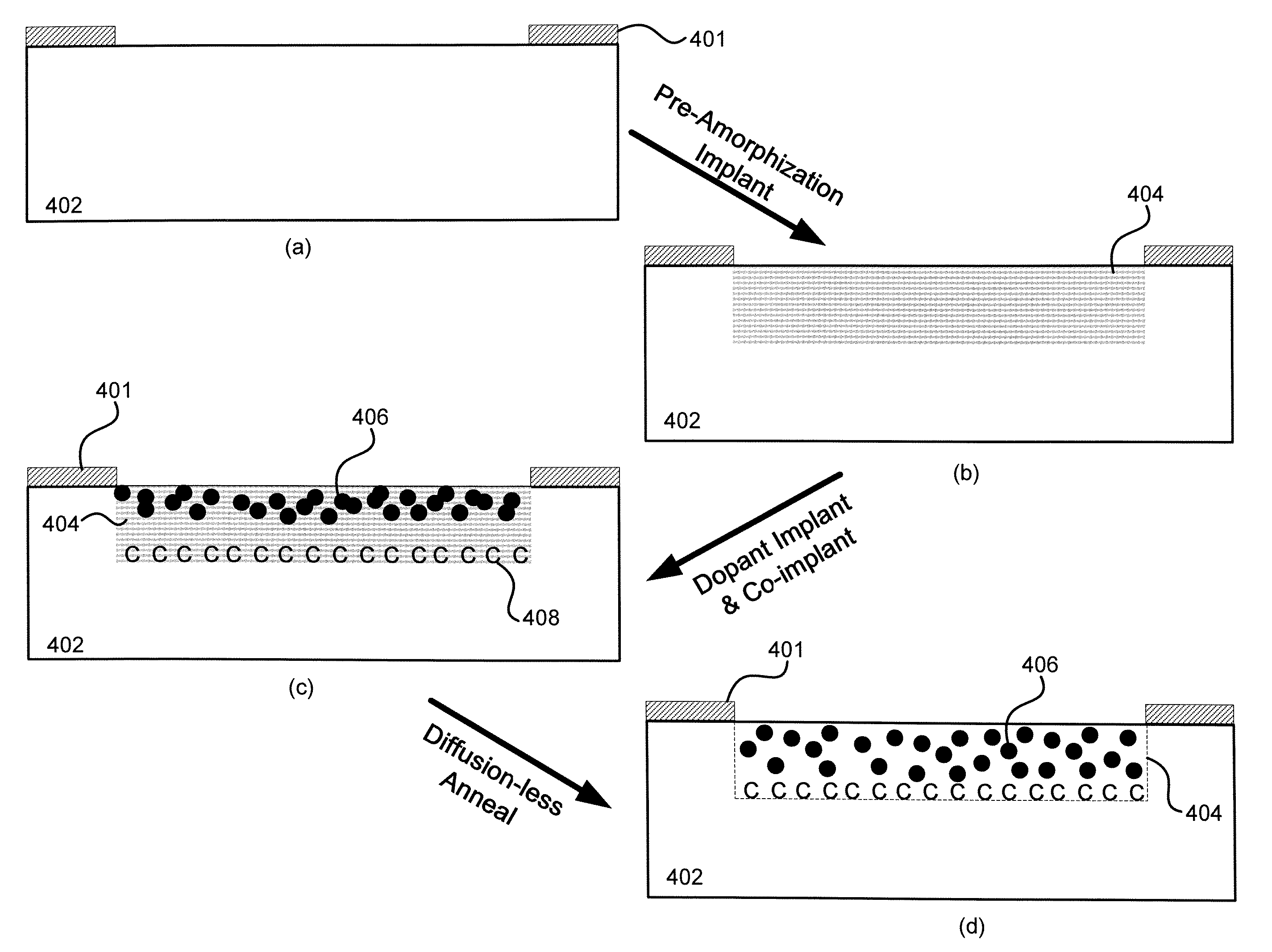
[0030]Embodiments of the present disclosure may reduce undesired migration of ion-implanted dopants through one or more auxiliary ion implantation processes. Prior to dopant implantation, a pre-amorphization implantation (PAI) may be performed on a target wafer with a molecular ion beam generated from one or more germanium-containing molecules. In addition to the dopant implantation, carbon- or fluorine-containing molecular ions may be co-implanted to place carbon or fluorine species into desired portions of the target wafer to mitigate TED effects. In some embodiments, the PAI and co-implant steps may be merged into one if a suitable molecular ion species is employed.

[0031]The techniques disclosed herein are not limited to beam-line ion implanters, but are also applicable to other types of ion implanters such as those used for plasma doping (PLAD) or plasma immersion ion implantation (PIII).

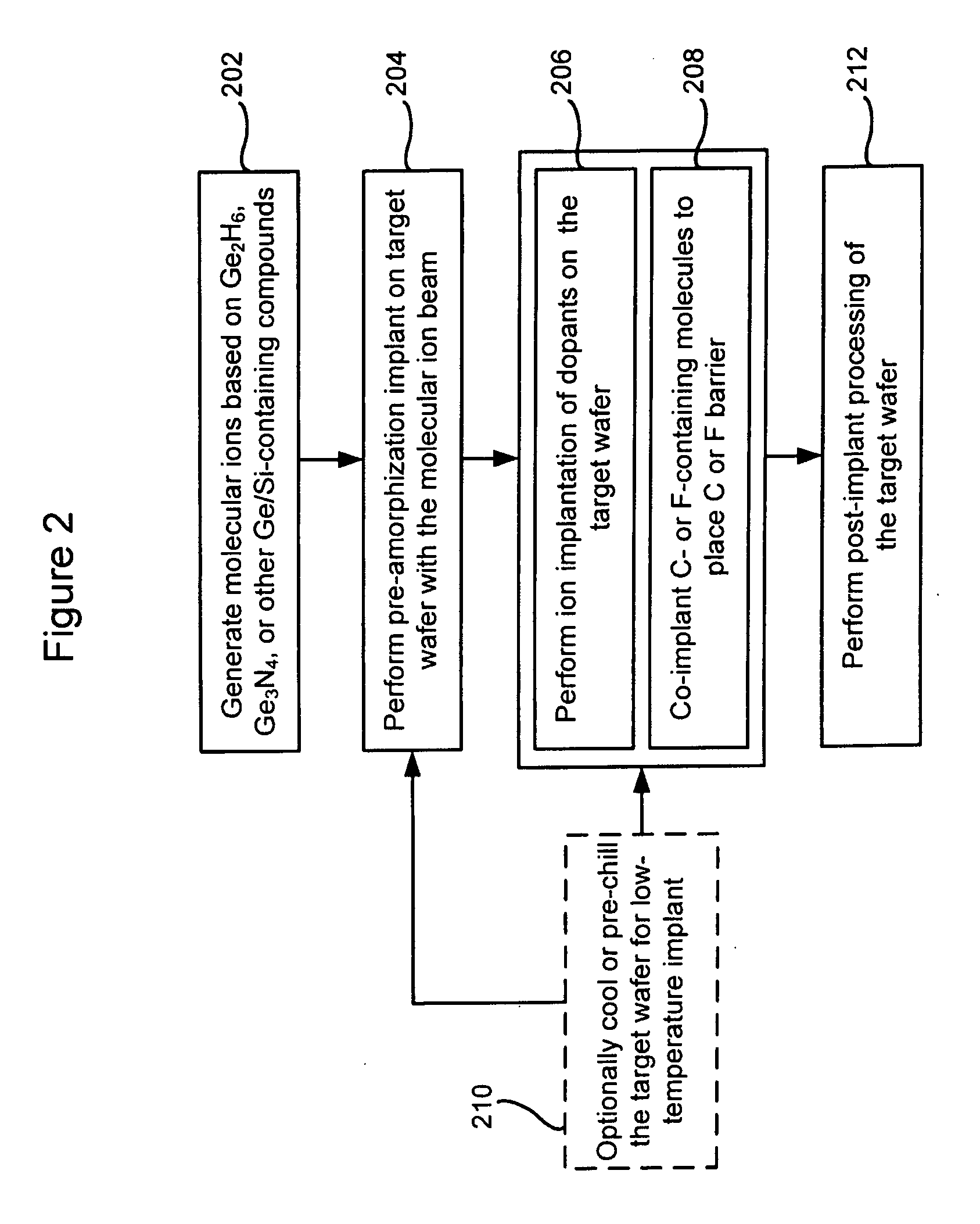
[0032]Referring to FIG. 2, there is shown a flow chart illustrating an exemplary method of f...


PUM


Abstract

Techniques for forming shallow junctions are disclosed. In one particular exemplary embodiment, the techniques may be realized as a method for forming shallow junctions. The method may comprise generating an ion beam comprising molecular ions based on one or more materials selected from a group consisting of: digermane (Ge2H6), germanium nitride (Ge3N4), germanium-fluorine compounds (GFn, wherein n=1, 2, or 3), and other germanium-containing compounds. The method may also comprise causing the ion beam to impact a semiconductor wafer.

Description

CROSS-REFERENCE TO RELATED APPLICATIONS[0001]This patent application claims priority to U.S. Provisional Patent Application No. 60 / 857,954, filed Nov. 8, 2006, which is hereby incorporated by reference herein in its entirety.[0002]This patent application is related to U.S. patent application Ser. No. 11 / 342,183, filed Jan. 26, 2006, which is hereby incorporated by reference herein in its entirety.FIELD OF THE DISCLOSURE[0003]The present disclosure relates generally to semiconductor manufacturing and, more particularly, to techniques for forming shallow junctions.BACKGROUND OF THE DISCLOSURE[0004]Ion implantation is a process of depositing chemical species into a substrate by direct bombardment of the substrate with energized ions. In semiconductor manufacturing, ion implanters are used primarily for doping processes that alter the type and level of conductivity of target materials. A precise doping profile in an integrated circuit (IC) substrate and its thin-film structure is often ...

Claims


Application Information

Patent Timeline
IPC IPC(8): H01L21/425
CPCH01J2237/2001H01J2237/31701H01L21/26593H01L21/26513H01L21/2658H01L21/26506H01L21/02592H01J37/08
Inventor AREVALO, EDWIN A.HATEM, CHRISTOPHER R.RENAU, ANTHONYENGLAND, JONATHAN GERALD
Owner VARIAN SEMICON EQUIP ASSOC INC
Why Eureka
Try Eureka