Pulsed ion beam control of solid state features

a technology of solid state structure and ion beam, which is applied in the direction of fluid speed measurement, chemical vapor deposition coating, lapping machine, etc., can solve the problems of inability to reproduce or predictably control the requisite nano-scale features, inability to control on a time scale commensurate with the time scale, and inability to manufacture many systems that include nano-metric feature dimensions and/or tolerances. practicable or economical,

Inactive Publication Date: 2006-10-10
PRESIDENT & FELLOWS OF HARVARD COLLEGE
View PDF36 Cites 126 Cited by
  • Summary
  • Abstract
  • Description
  • Claims
  • Application Information

AI Technical Summary

Problems solved by technology

But in the fabrication of many nano-regime systems, in which structural feature dimensions of a few nanometers are of importance, it is generally found that conventionally-proposed techniques often cannot form the requisite nano-scale features reproducibly or predictably, and often cannot be controlled on a time scale commensurate with production of such nano-scale features.
As a result, volume manufacture of many systems that include nanometric feature dimensions and / or tolerances is not practical or economical.

Method used


Image

  • Pulsed ion beam control of solid state features
  • Pulsed ion beam control of solid state features
  • Pulsed ion beam control of solid state features

Examples


example 1

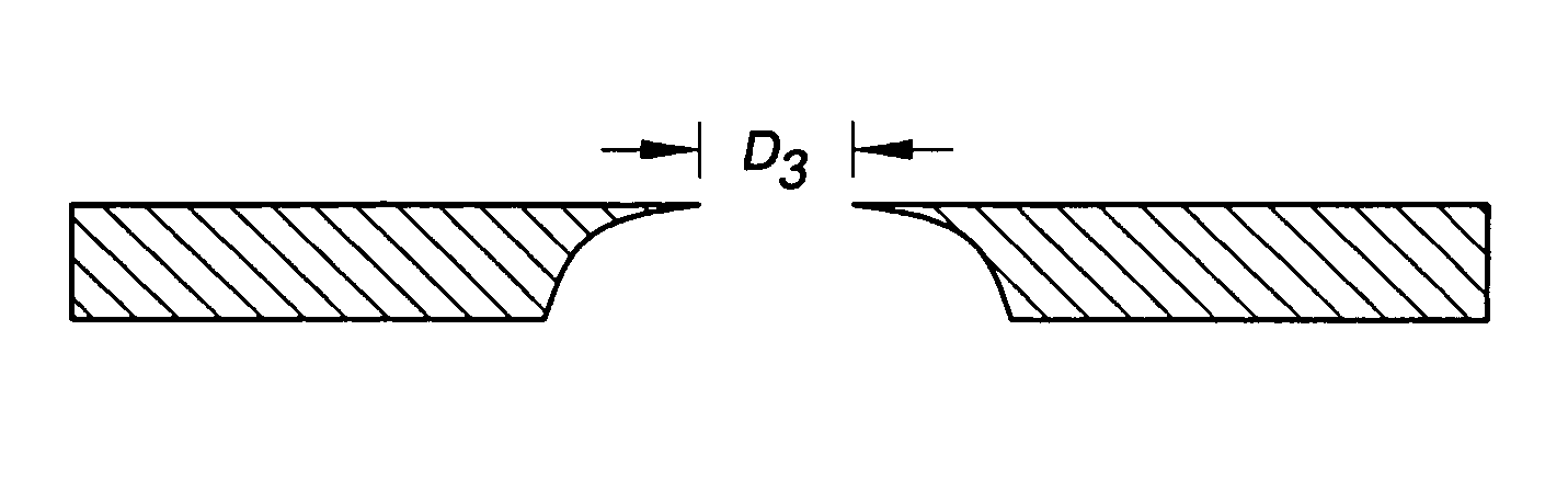
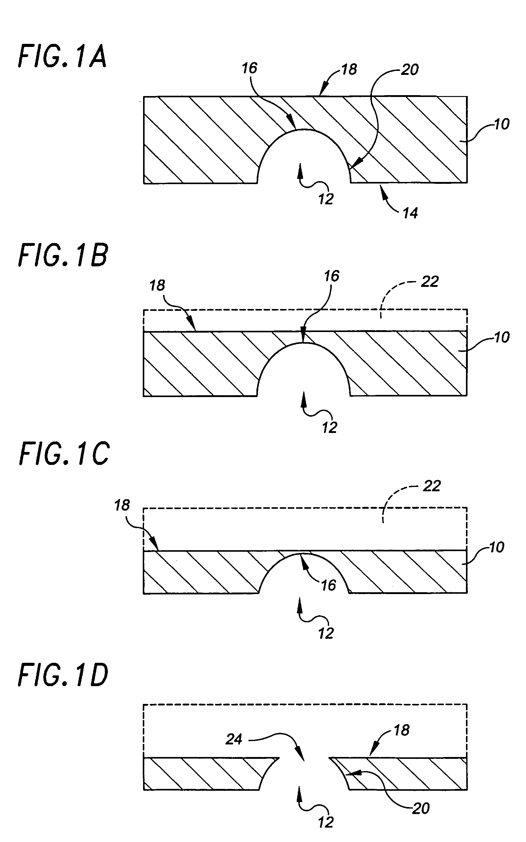
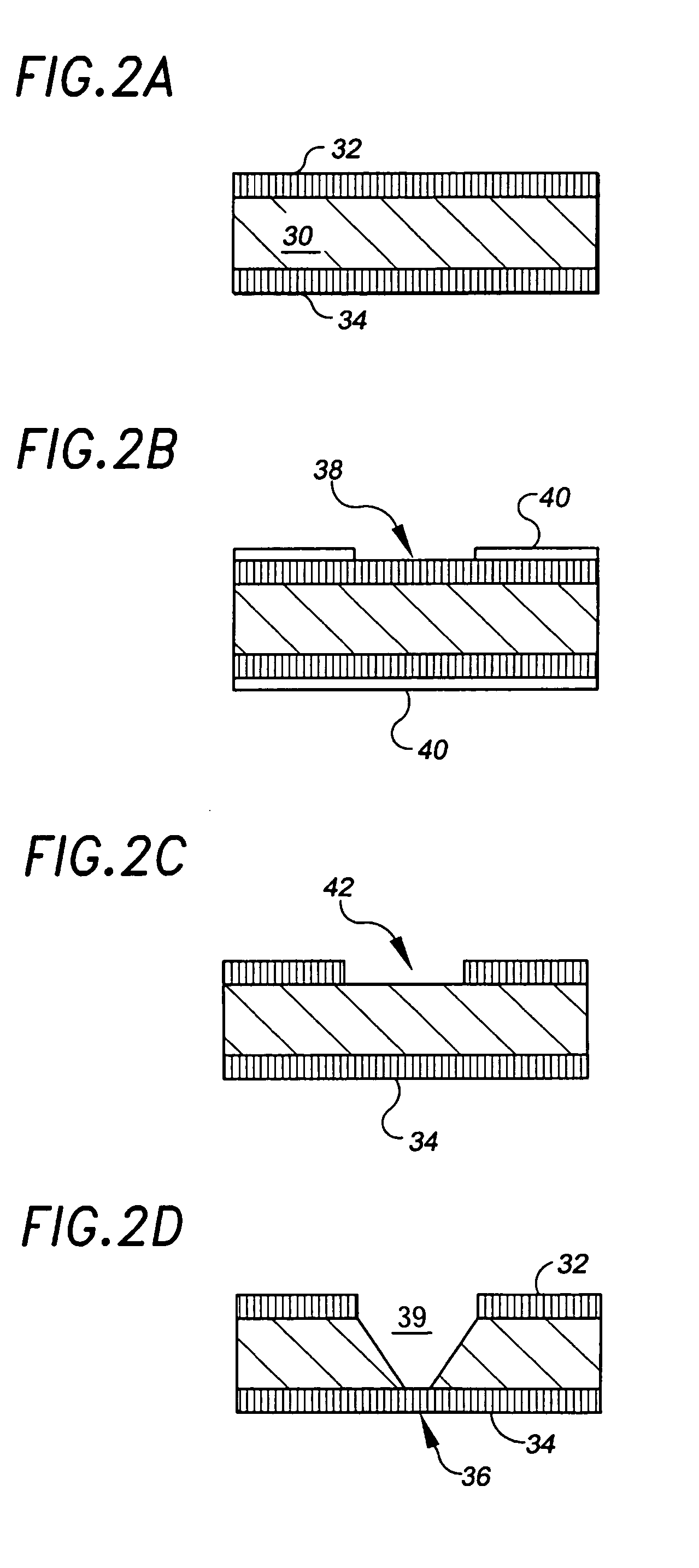
[0078]A 50 nm-thick silicon nitride membrane having a cavity formed on one surface was produced by the process outlined in FIGS. 2A–G. The silicon nitride was deposited by low pressure chemical vapor deposition. The cavity bowl was etched in the membrane by a reactive ion etch process. FIG. 4A is an electron micrograph of the cavity formed in the membrane.

[0079]The membrane surface opposite that including the cavity was exposed to an argon ion beam etch at an energy of about 3 KeV, and a flux of about 3 Ar+sec / nm2. The ion beam diameter was about 200 μm and the membrane temperature during the etch was maintained at about −120° C. The ion beam was directed toward the membrane for 1 sec during each 5 sec interval. During the etch process, ion detection and counting was carried out.

[0080]FIG. 4B is an electron micrograph of the membrane cavity including a 10 nm limiting aperture formed by thinning of the membrane. FIG. 4C is a plot of argon ion count / second as a function of sputtering ...

example 2

[0091]A silicon nitride membrane of about 50 nm in thickness was produced in the manner of FIGS. 2A–2E. An aperture was formed through the entire thickness of the membrane by reactive ion etch. This resulted in a 37 nm-wide aperture, an electron micrograph of which is shown in FIG. 5A. The membrane and aperture were then exposed to an argon ion beam at a flux of about 1.7 Ar+ / nm2 / sec and an energy of about 3 KeV. The ion beam was directed toward and away from the membrane to sputter for 1 second during each 5 second interval. The membrane was maintained at a temperature of about −102° C. during the ion beam exposure.

[0092]FIG. 5B is an electron micrograph of the 58 nm-wide aperture that resulted from 180 seconds of sputtering. FIG. 5C is a plot of counted ions / sec as a function of time. A generally linear relationship between ion counts as a function of time is demonstrated.

[0093]The invention does not require that the process being controlled by feedback be a subtractive process as...

example 3

[0099]A silicon nitride membrane of about 500 nm in thickness was produced in the manner of the process outlined in FIGS. 2A–E. An aperture was formed through the entire thickness of the membrane by reactive ion etching. FIG. 7A is an electron micrograph of the 95 nm-wide aperture that resulted from the etch.

[0100]The membrane and its aperture were then exposed to an argon ion beam flux at an energy of about 3 KeV, and a flux of about 47 Ar+ / sec / nm2. The membrane was maintained at a temperature of about 20° C. during ion flux exposure. The ion beam was directed to the membrane for 250 ms for each 1 sec time interval.

[0101]FIG. 7B is an electron micrograph of the membrane after exposure to the argon ion beam reduced the aperture diameter to about 3 nm. FIG. 7C is a plot of counted argon ions / sec as a function of time. A generally linear count rate is indicated for midpoints in the process.

[0102]Without being bound by theory, the inventors herein understand that the mechanisms underly...


PUM

PropertyMeasurementUnit
widthaaaaaaaaaa
widthaaaaaaaaaa
thicknessaaaaaaaaaa

Abstract

For controlling a physical dimension of a solid state structural feature, a solid state structure is provided, having a surface and having a structural feature. The structure is exposed to a first periodic flux of ions having a first exposure duty cycle characterized by a first ion exposure duration and a first nonexposure duration for the first duty cycle, and then at a second periodic flux of ions having a second exposure duty cycle characterized by a second ion exposure duration and a second nonexposure duration that is greater than the first nonexposure duration, for the second duty cycle, to cause transport, within the structure including the structure surface, of material of the structure to the structural feature in response to the ion flux exposure to change at least one physical dimension of the feature substantially by locally adding material of the structure to the feature.

Description

[0001]This application claims the benefit of U.S. Provisional Application No. 60 / 421,908 filed Oct. 29, 2002, the entirety of which is hereby incorporated by reference. This application is a continuation-in-part U.S. Non-provisional application Ser. No. 10 / 186,105, filed Jun. 27, 2002, now issued as U.S. Pat. No. 6,783,643, which claims the benefit of U.S. Provisional Application No. 60 / 301,400, filed Jun. 27, 2001, the entirety of which is hereby incorporated by reference, and is a continuation-in-part of U.S. Non-provisional application Ser. No. 09 / 599,137, filed Jun. 22, 2000, now issued as U.S. Pat. No. 6,464,842, which claims the benefit of U.S. Provisional Application No. 60 / 140,201, filed Jun. 22, 1999, the entirety of which is hereby incorporated by reference.CROSS REFERENCE TO RELATED APPLICATION[0002]This application is related to U.S. Non-provisional application Ser. No. 09 / 602,650, now issued as U.S. Pat. No. 6,627,067, entitled “Molecular and Atomic Scale Evaluation of ...

Claims


Application Information

Patent Timeline
Patent Type & Authority Patents(United States)
IPC IPC(8): C23C14/00B01L3/00B81B1/00B81C1/00B81C99/00G01N27/28G01N27/416H01L21/66
CPCB24B37/013B81C1/00626B81C99/004G01N33/48721H01L22/26B01L3/5027B81C2201/0143H01L2924/0002H01L2924/00
Inventor GOLOVCHENKO, JENE A.STEIN, DEREK M.LI, JIALI
Owner PRESIDENT & FELLOWS OF HARVARD COLLEGE
Why Eureka
Try Eureka