
Membrane die attach circuit element package and method therefor

Active Publication Date: 2010-08-24
AMKOR TECH SINGAPORE HLDG PTE LTD
View PDF19 Cites 43 Cited by
  • Summary
  • Abstract
  • Description
  • Claims
  • Application Information

AI Technical Summary

Benefits of technology

[0005]A circuit element package has a substrate having a plurality of electrically conductive patterns, a die pad, and an access hole formed through the die pad and substrate. A plurality of leads is coupled to the substrate. A circuit element die is attached to the die pad wherein a first sensor port is positioned over the access hole. A die attach membrane is provided for attaching the circuit element die to the die pad. The die attach membrane allows the circuit element die to sense ambient while protecting the circuit element die from environmental damage. An encapsulant is used for covering portions of the circuit element die.

Problems solved by technology

However, by isolating the sensing element from the ambient environment, a certain degree of accuracy is lost.
Furthermore, in some pressure sensors, the material used to hold the sensing elements may not be resistant to the operating environment.
This may cause the pressure sensor to fail in a corrosive environment.

Method used


Image

  • Membrane die attach circuit element package and method therefor
  • Membrane die attach circuit element package and method therefor
  • Membrane die attach circuit element package and method therefor

Examples


Embodiment Construction

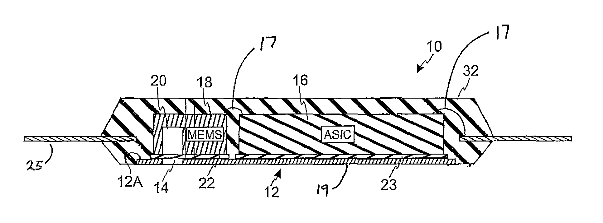
[0025]Referring to FIG. 1, a cross-sectional view of a circuit element package 10 is shown. In the embodiment of FIG. 1, the circuit element package 10 is a leadframe type of package. However, this should not be seen as to limit the scope of the present invention. The semiconductor device 10 may be a leaded type of device, a Ball Grid Array (BGA) type of device, a Land Grid Array (LGA) type of device, or the like.

[0026]The circuit element package 10 has a substrate 12. The substrate 12 is generally made of a metal material. Examples of the metal material include, but are not limited to: copper, copper alloy, plated copper, plated copper alloy, Alloy 37, steel plated with copper, and the like. The substrate 12 comprises a die pad 19 and a plurality of leads 25 positioned around the die pad 19. A die pad 19 is formed on the first surface 12A of the substrate 12. An access hole 14 is formed through the die pad 19 of the substrate 12.

[0027]A semiconductor die 16 and a circuit element di...


PUM


Abstract

A circuit element package has a substrate having a plurality of electrically conductive patterns, a die pad, and an access hole formed through the die pad and substrate. A plurality of leads is coupled to the substrate. A circuit element die is attached to the die pad wherein a first sensor port is positioned over the access hole. A die attach membrane is provided for attaching the circuit element die to the die pad. The die attach membrane allows the circuit element die to sense ambient while protecting the circuit element die from environmental damage. An encapsulant is used for covering portions of the circuit element die.

Description

FIELD OF THE INVENTION[0001]This invention relates to a circuit element package and, more specifically, to a circuit element package having a membrane element which enables a circuit element die to be exposed to the ambient the circuit element die is to measure, while also protecting the circuit element die from destructive environmental agents.BACKGROUND OF THE INVENTION[0002]Sensor applications are expanding rapidly. This is especially true in the Micro-Electro-Mechanical System (MEMS) field. The MEMS field is the integration of mechanical elements, sensors, actuators, or the like and electronics on a common silicon substrate through microfabrication technology.[0003]Presently, the packaging of pressure sensors typically includes isolating the sensing element from the ambient environment. However, by isolating the sensing element from the ambient environment, a certain degree of accuracy is lost. Furthermore, in some pressure sensors, the material used to hold the sensing elements...

Claims


Application Information

Patent Timeline
IPC IPC(8): G01L9/04
CPCG01L19/0636G01L19/141G01L19/147H01L2924/1461H01L2924/1815H01L2924/15311H01L2224/73265H01L2224/48465H01L2224/48247H01L2224/48227H01L2224/48137H01L2224/48091H01L2224/32225H01L2924/00014H01L2924/00H01L2924/181H01L2924/15151H01L2924/00012
Inventor FAHEEM, FAHEEM F.SCANLAN, CHRISTOPHER M.BERRY, CHRISTOPHER J.
Owner AMKOR TECH SINGAPORE HLDG PTE LTD
Features
  • Generate Ideas
  • Intellectual Property
  • Life Sciences
  • Materials
  • Tech Scout
  • Unparalleled Data Quality
  • Higher Quality Content
  • 60% Fewer Hallucinations
Learn More