Light emitting device and driving method of the same

a technology of light emitting devices and driving methods, applied in static indicating devices, instruments, organic semiconductor devices, etc., can solve the problems of low power consumption, degrade image quality, and emitting elements, and achieve the effect of enhancing the brightness of display colors and image contrast, and reducing the load on each light emitting elemen

Inactive Publication Date: 2010-09-07
SEMICON ENERGY LAB CO LTD
View PDF38 Cites 74 Cited by
  • Summary
  • Abstract
  • Description
  • Claims
  • Application Information

AI Technical Summary

Benefits of technology

[0006]The invention provides a light emitting device of which luminance decay caused with the light emission time or by the light emission at a high luminance can be decreased. Moreover, the invention relates to a driving method which can suppress the reduction of luminance in accordance with the light emission time and light emission at a high luminance.
[0012]According to the invention, a light emitting device which exhibits white light emission can be provided. By performing a white light emission, the luminance of the display color and the contrast of an image can be enhanced. Accordingly, for example, when forming a display color by mixing light emission of red, green, and blue light emitting elements, load imposed on each light emitting element can be reduced, leading to a long life of the light emitting element.

Problems solved by technology

A light emitting device using light emission of an electroluminescence element (light emitting element) is wide in viewing angle and low in power consumption.
Such a luminance decay causes the change in display color of the light emitting device which functions as a display device, leading to degrade the image quality.

Method used


Image

  • Light emitting device and driving method of the same
  • Light emitting device and driving method of the same
  • Light emitting device and driving method of the same

Examples


embodiment mode 1

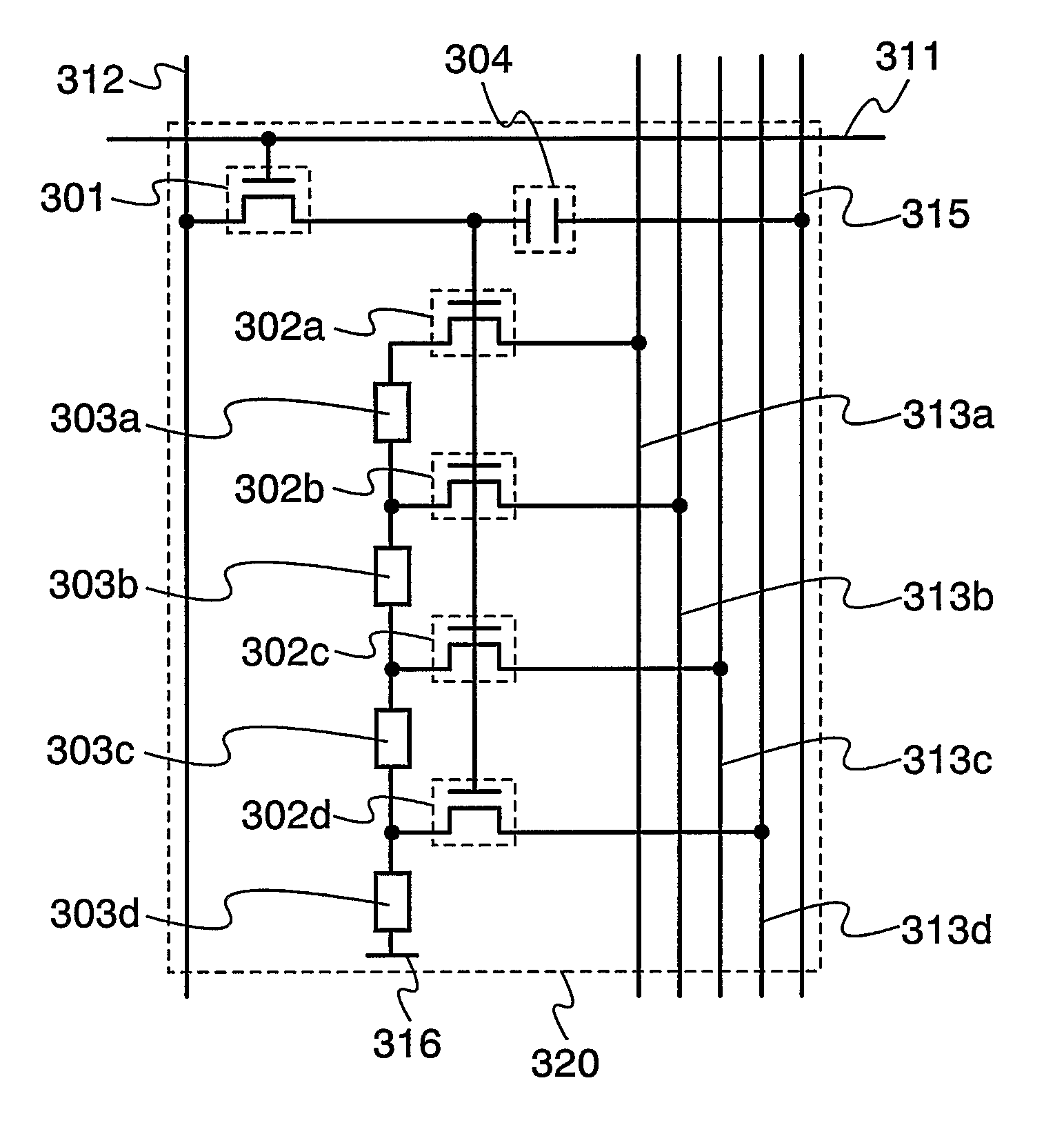
[0025]A circuit included in a pixel portion of the light emitting device of the invention is described with reference to FIG. 1.

[0026]FIG. 1 is a diagram showing a circuit configuration of a pixel 320 included in the light emitting device of the invention.

[0027]A switching transistor 301, driving transistors 302a, 302b, 302c, and 302d each has three terminals: a gate electrode, a drain region, and a source region, in which a channel region is provided between the drain region and the source region. Here, the source region and the drain region cannot be clearly distinguished because of the structure, operating condition, and the like of the transistor, therefore, one of them is referred to as a first electrode while the other is referred to as a second electrode. Here, a switching transistor controls a video signal input to a driving transistor. The driving transistor determines light emission or no light emission of a light emitting element by controlling a current supply from a cur...

embodiment mode 2

[0034]In this embodiment mode, the light emitting device of the invention including a pixel having the circuit configuration described in Embodiment Mode 1 and a driving method thereof are described.

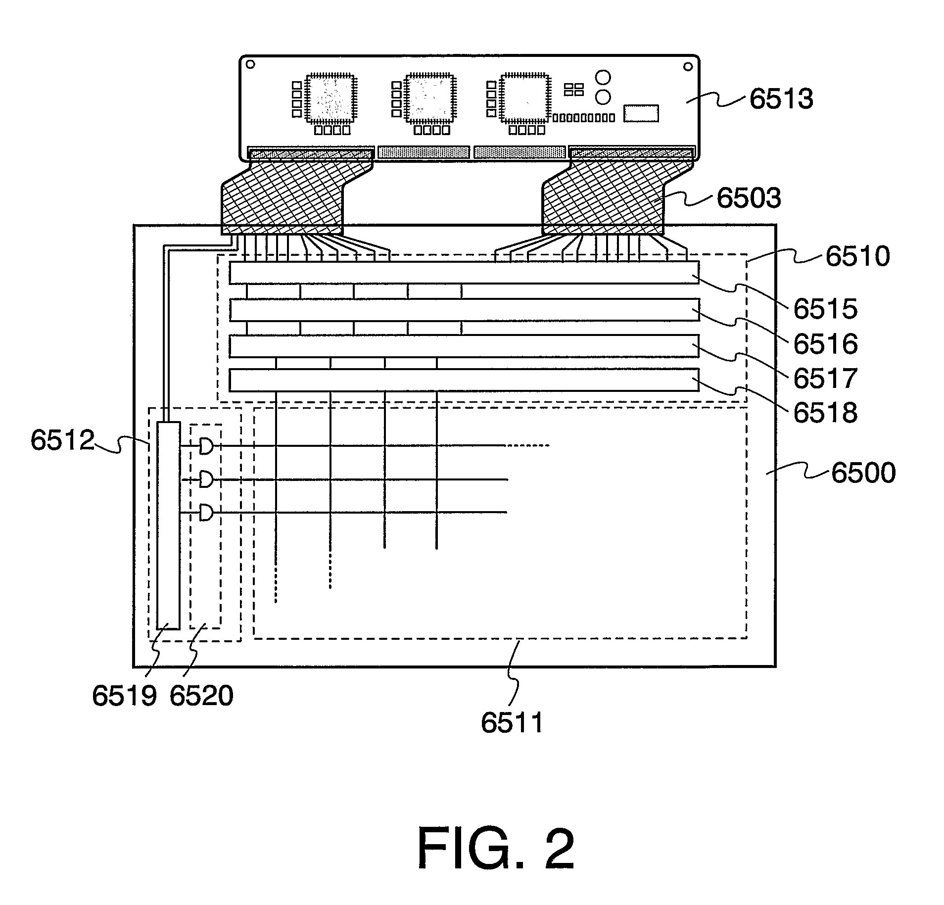
[0035]FIG. 2 is a schematic diagram of a light emitting device seen from the top, to which the invention is applied. In FIG. 2, a region 6510 surrounded by a dotted line denotes a driver circuit portion (a source driver circuit), a region 6511 denotes a pixel portion, and a region 6512 denotes a driver circuit portion (a gate driver circuit). The pixel portion 6511 is provided with the light emitting element of the invention. The driver circuit portions 6510 and 6512 are connected to an FPC 6503 as an external input terminal through wirings formed on a substrate 6500. The driver circuit portions 6510 and 6512 are inputted with signals by receiving a video signal, a clock signal, a start signal, a reset signal and the like from the FPC (Flexible Printed Circuit) 6503. A printed wiring boa...

embodiment mode 3

[0047]In this embodiment mode, a driving method of the light emitting device of the invention is described, which is different than the driving method thereof described in Embodiment Mode 2. It is to be noted that a similar circuit configuration of a pixel portion to that described in Embodiment Mode 2 can be used. In this embodiment mode also, reference numerals shown in FIG. 3 are referred to.

[0048]Hereinafter described with reference to FIGS. 5A and 5B is an operation of the light emitting device of this embodiment mode. FIGS. 5A and 5B are diagrams showing operations of frames with time. FIG. 5B is a diagram showing the operation of the frame with time in a first subframe of a plurality of subframes in one frame. In FIG. 5B, the lateral direction denotes time while the longitudinal direction denotes a scan stage of the gate signal line.

[0049]According to the light emitting device of this embodiment mode, one frame is divided into four first subframes 601, 602, 603, and 604 by ti...


PUM


Abstract

The invention provides a light emitting device which can suppress the reduction of luminance in accordance with the light emission time and light emission at a high luminance. Moreover, the invention relates to a driving method which can suppress the reduction of luminance in accordance with the light emission time and light emission at a high luminance. The light emitting device of the invention can display a plurality of colors of which brightness and chromaticity are different by visually mixing light emission of a plurality of light emitting elements of which light emission colors are different. When a visually mixed display color is formed, a white light emission is exhibited.

Description

TECHNICAL FIELD[0001]The present invention relates to a light emitting device which displays colors using light emission of a light emitting element, and a driving method thereof.BACKGROUND ART[0002]A light emitting device using light emission of an electroluminescence element (light emitting element) is wide in viewing angle and low in power consumption. In recent years, a light emitting device which can provide high quality images has been actively researched and developed in view of capturing a market as a display device applicable to various information processing devices such as a television receiver and a car navigation system.[0003]The luminance of the light emitting element decays with light emission time. Such a decay becomes notable when the light emitting element keeps emitting light at a high luminance. Such a luminance decay causes the change in display color of the light emitting device which functions as a display device, leading to degrade the image quality.[0004]The...

Claims


Application Information

Patent Timeline
Patent Type & Authority Patents(United States)
IPC IPC(8): G09G3/30G09G3/32G09G3/20H01L27/32H05B33/14
CPCH01L27/3209G09G3/2022G09G3/2025G09G2300/0452G09G2300/0465G09G2300/0842H01L2251/562G09G2320/043G09G2330/02H01L27/3244G09G2310/0235H10K59/32H10K59/12H10K71/831G09G3/30G09G3/32G09G3/20H05B33/14
Inventor OHTANI, HISASHITANADA, YOSHIFUMIANZAI, AYA
Owner SEMICON ENERGY LAB CO LTD
Why Eureka
Try Eureka