
Solid-state imaging apparatus

a solid-state imaging and apparatus technology, applied in the direction of television system scanning details, radioation controlled devices, television systems, etc., can solve the problems of easy degradation of the transfer efficiency of the signal charge input to the ccd register, difficult layout design of the ccd register, and increase the area of the solid-state imaging apparatus, so as to prevent the increase of the area and the effect of deteriorating the transfer efficiency

Inactive Publication Date: 2010-10-05
RENESAS ELECTRONICS CORP
View PDF4 Cites 0 Cited by
  • Summary
  • Abstract
  • Description
  • Claims
  • Application Information

AI Technical Summary

Benefits of technology

[0012]The solid-state imaging apparatus of the present invention enables prevention of the increase of the area of the solid-state imaging apparatus and deterioration of the transfer efficiency.

Problems solved by technology

Therefore, there is a problem that the area of the solid-state imaging apparatus increases.
In this case, as the CCD register is folded back by 90 degrees, it is difficult to layout design of the CCD register.
Further, transfer efficiency of the signal charge input to the CCD register is easy to worsen.

Method used


Image

  • Solid-state imaging apparatus
  • Solid-state imaging apparatus
  • Solid-state imaging apparatus

Examples


first embodiment

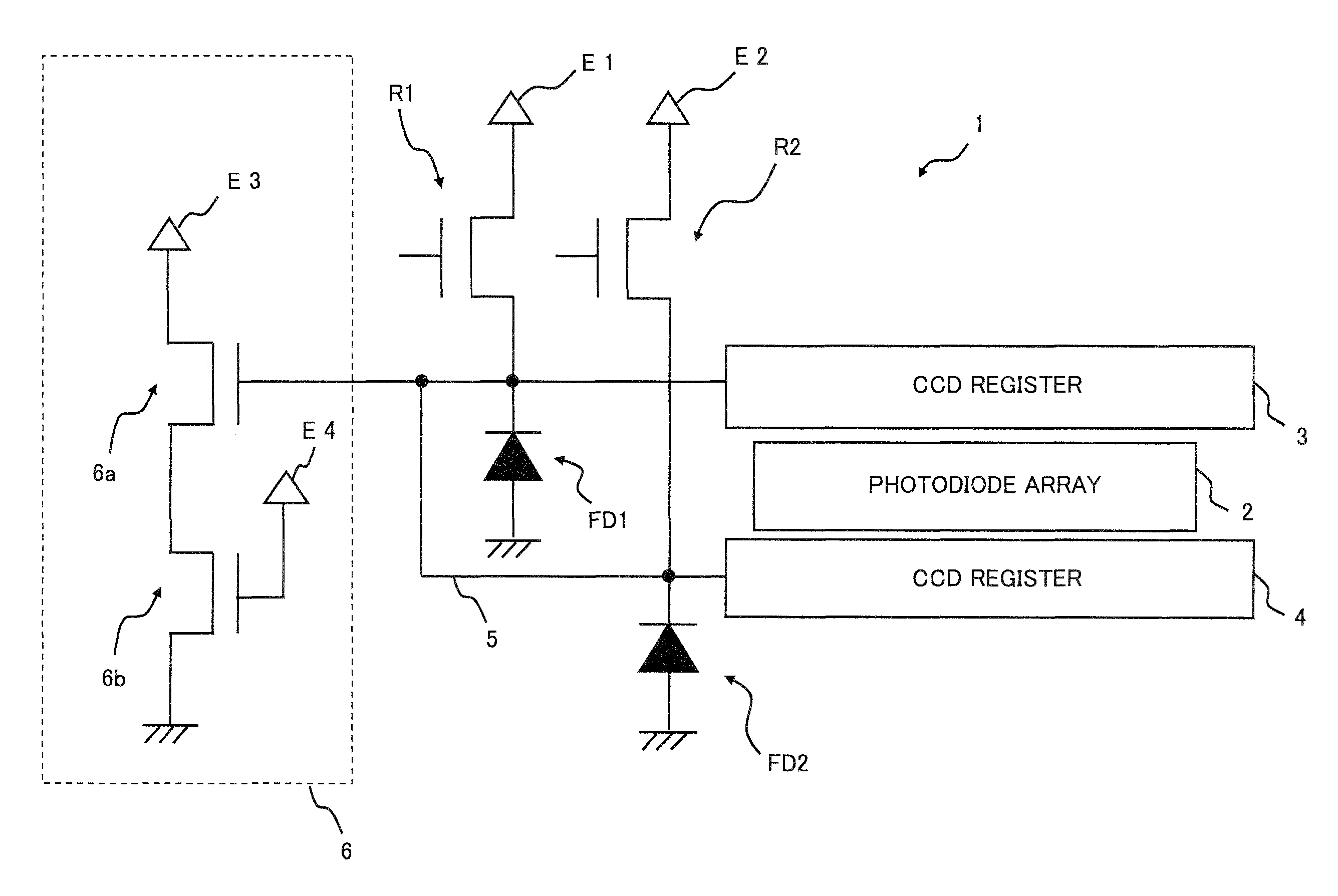
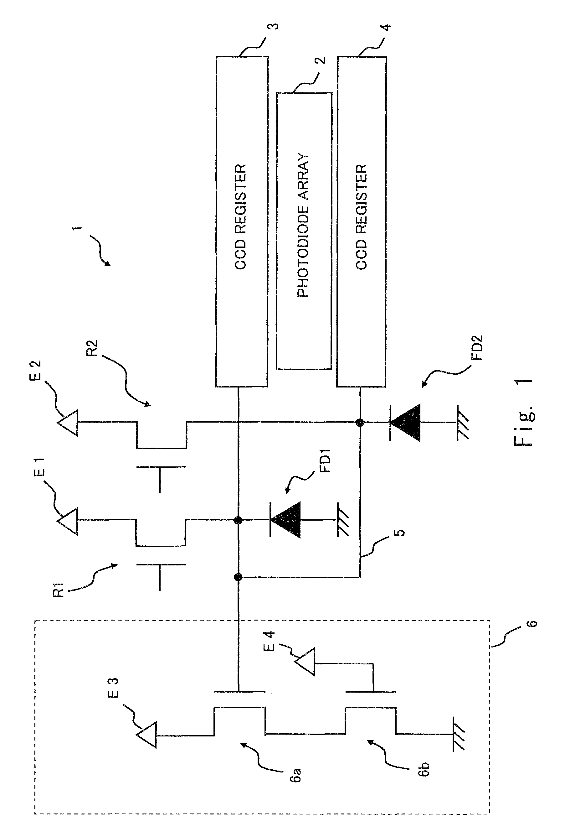
[0022]A first embodiment of the present invention is described hereinafter with reference to FIG. 1. FIG. 1 is a schematic diagram of a solid-state imaging apparatus 1 according to this embodiment. As shown in FIG. 1, the solid-state imaging apparatus 1 includes a photodiode array 2 (a pixel array), a CCD register 3 (a first charge transfer unit), a CCD register 4 (a second charge transfer unit), floating diffusions FD1 and FD2 (first and second floating diffusion regions), a metal wiring 5 (a wiring layer), an output circuit 6, reset transistors R1 and R2, and a plurality of constant-voltage sources E1 to E4. The structure of the solid-state imaging apparatus 1 is described hereinafter in detail.

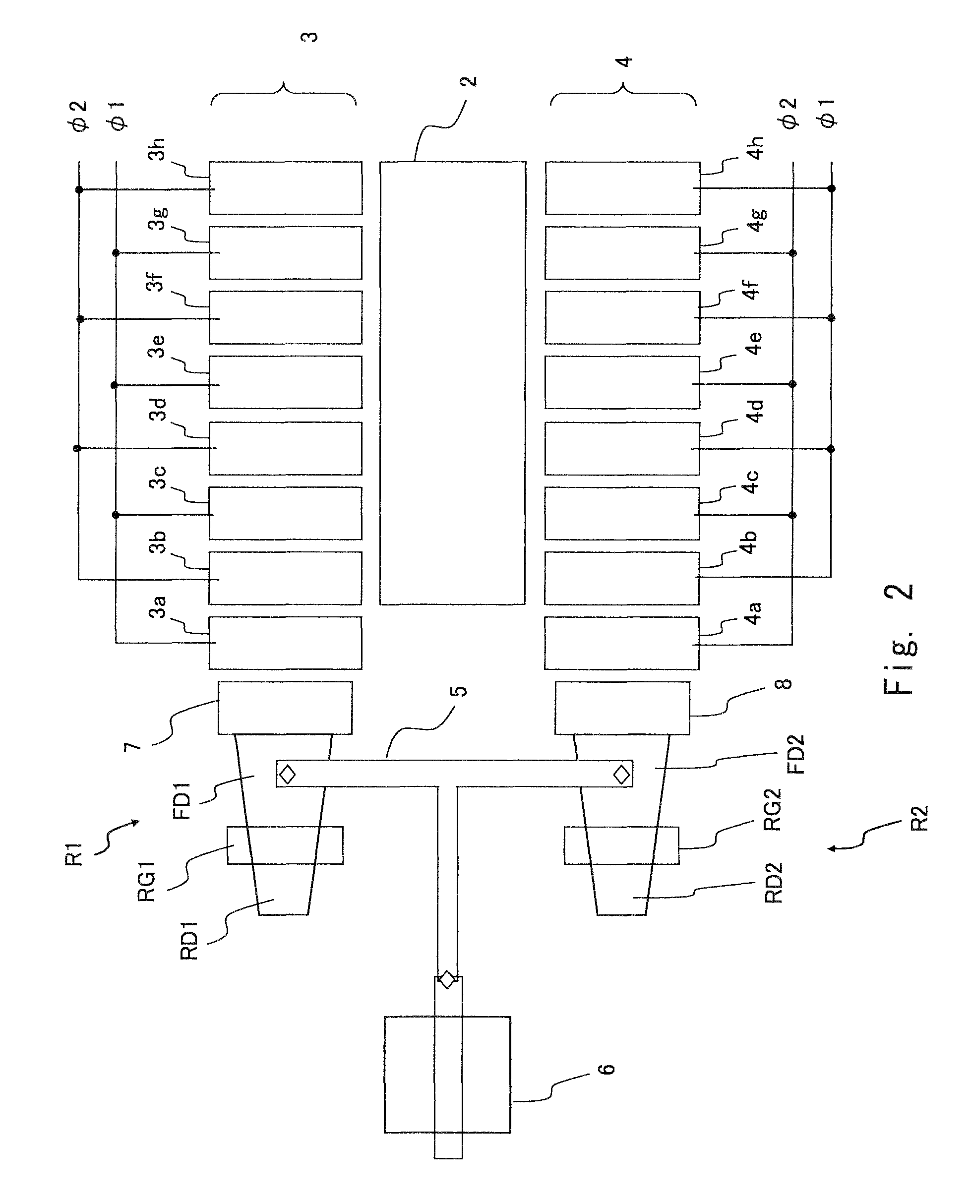
[0023]The CCD register 3 and the CCD register 4 are each arranged on each side of the photodiode array (the pixel array) 2. In the photodiode array 2, a light receiving element such as a plurality of the photodiodes (pixels) is disposed in a charge transfer direction (not shown). The CCD re...

second embodiment

[0032]Next, second embodiment of the present invention is described hereinafter. In the first embodiment, the floating diffusion FD1 is connected to the reset transistor R1, and the floating diffusion FD2 is connected to the reset transistor R2. In the second embodiment, to achieve further miniaturization and to raise the sensitivity of the solid-state imaging apparatus, only one reset transistor is formed instead of forming the reset transistor which is connected to each of the floating diffusion FD1 and the floating diffusion FD2. The solid-state imaging apparatus 10 in this embodiment is shown in FIG. 4. In the second embodiment, the same elements as in the first embodiment are denoted by the same reference symbols, and the details thereof are omitted.

[0033]As shown in FIG. 4, the floating diffusion FD1 and the floating diffusion FD2 are commonly connected to the reset transistor R3. The floating diffusion FD1 and the floating diffusion FD2 are connected to each other by the meta...


PUM


Abstract

A solid-state imaging apparatus includes a pixel array comprising a plurality of light receiving elements disposed in a charge transfer direction, the plurality of light receiving elements converting a light signal into an electric signal, a first charge transfer unit and a second charge transfer unit arranged on each side of the pixel array and transferring a signal charge input from the pixel array in the charge transfer direction, a first floating diffusion region connected to the first charge transfer unit, a second floating diffusion region connected to the second charge transfer unit, a wiring layer connecting the first floating diffusion region with the second floating diffusion region, and an output circuit connected to the wiring layer and output a signal voltage in accordance with a potential of the first floating diffusion region and the second floating diffusion region.

Description

BACKGROUND OF THE INVENTION[0001]1. Field of the Invention[0002]The present invention relates to a solid-state imaging apparatus, and, more specifically, to a linear image sensor having a pixel array in which a plurality of receiving elements are disposed along a charge transfer direction and of which a plurality of CCD registers are arranged on each side.[0003]2. Description of Related Art[0004]A linear image sensor transfers a signal charge which is stored in a light receiving element such as a photodiode via a CCD (Charge Coupled Device) register and outputs the signal charge which is converted to a voltage. The linear image sensor which has CCD registers arranged on each side of a photodiode (pixel) array is often used, because it is easy to be designed. The Staggered structure is also often used. The Staggered structure has a plurality of pixel arrays which is shifted by ½, ⅓, ¼ . . . pixel pitches. By having such a structure, the liner image sensor can be high-resolution.[0005...

Claims


Application Information

Patent Timeline
Patent Type & Authority Patents(United States)
IPC IPC(8): H01L27/148H01L29/768H04N1/028H04N5/335H04N5/369H04N5/372
CPCH04N3/1575H04N3/1581H01L27/148H04N25/701H04N25/713
Inventor UEMURA, AKIRA
Owner RENESAS ELECTRONICS CORP
Learn More