Eureka AIR delivers breakthrough ideas for toughest innovation challenges, trusted by R&D personnel around the world.

Non-volatile memory control device

a non-volatile memory and control device technology, applied in the direction of digital storage, electric digital data processing, instruments, etc., can solve the problems of deteriorating writing reliability, difficult to secure the execution timing of additional writing operations, etc., and achieve the effect of reducing data writing tim

Active Publication Date: 2010-10-05
CETUS TECH INC
View PDF10 Cites 2 Cited by
  • Summary
  • Abstract
  • Description
  • Claims
  • Application Information

AI Technical Summary

Benefits of technology

[0022]Therefore, a main object of the present invention is to provide a non-volatile memory control device capable of securing the timing of the execution of the additional writing operation even in the case where a large volume of data is written at a high speed, and thereby reducing the data writing time and assuring the writing reliability at the same time.
[0033]According to the present invention, an additional writing instruction is given to one of the non-volatile memories waiting for a writing operation, while a temporarily writing instruction is given to another non-volatile memory. More specifically, while an additional writing operation is being executed to one of the non-volatile memories, a temporary writing operation is executed at least once to another non-volatile memory. Accordingly, an amount of time in total necessary for the writing operations in the plurality of non-volatile memories can be cut down. The amount of time in total necessary for the writing operations in the plurality of non-volatile memories can be cut down further when the temporary writing operation is executed to one of the non-volatile memories at least twice while the additional writing operation is being executed to other non-volatile memory.
[0094]Accordingly, a writing durability, which may be deteriorated as the additional writing operation is executed more often, can last longer, and the reliability and service life can be thereby improved. In the case where it is unnecessary to retain the data for a long period of time in view of the conditions of the memory block and the contents of the data, the additional writing operation is not executed. As a result, the writing durability, which may be deteriorated as the additional writing operation is executed more often, can last longer, and the reliability and service life can be thereby improved.
[0095]According to the present invention, the execution timing of the additional writing operation can be assured even in the case where a large number of data is written at a high speed. As a result, the amount of time necessary for the memory controller to write the data in the non-volatile memories can be reduced, and the reliability and service life can be improved at the same time.
[0096]The non-volatile memory control device according to the present invention is advantageous in that the reduction of an amount of time necessary for data writing and improvements of the reliability and service life can be both achieved in a non-volatile memory (flash non-volatile memory, SD card memory, etc.).

Problems solved by technology

When a large volume of data is written at a high speed in the conventional EEPROM from the memory-controller side, there arise a too large number of memory blocks in the memory cell array already subjected to the temporary writing operation, which makes it difficult to secure an execution timing of the additional writing operation.
As a result, the execution of the additional writing operation fails in some of the memory blocks, and the data writing performance cannot be as solid as expected, which deteriorates the writing reliability.

Method used


Image

  • Non-volatile memory control device
  • Non-volatile memory control device
  • Non-volatile memory control device

Examples


embodiment 1

Preferred Embodiment 1

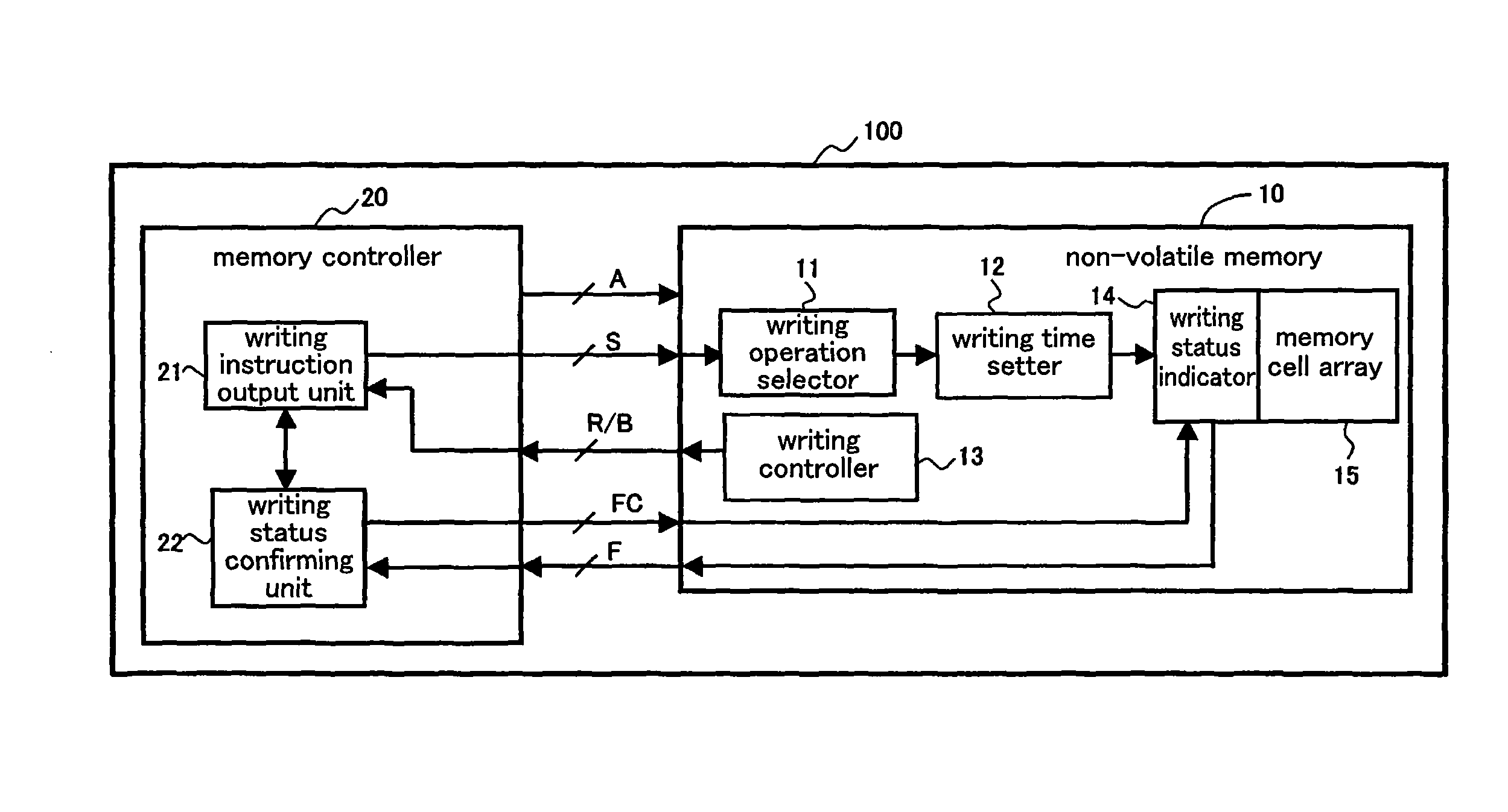
[0113]FIG. 1 is a block diagram illustrating a constitution of a non-volatile memory control device 100 according to a preferred embodiment 1 of the present invention. The non-volatile memory control device 100 according to the preferred embodiment 1 comprises a non-volatile memory 10, such as EEPROM, and a memory controller 20 which controls a writing operation in the non-volatile memory 10. The non-volatile memory 10 comprises a memory cell array divided into a plurality of memory blocks.

[0114]The non-volatile memory 10 comprises a writing operation selector 11, a writing time setter 12, a writing controller 13, a writing status indicator 14, and a memory cell array 15. A temporary writing instruction or an additional writing instruction is inputted to the writing operation selector 11 from the memory controller 20. The writing operation selector 11 selects one of a temporary writing operation in which data is written in the memory cell array 15 at a high spe...

embodiment 2

Preferred Embodiment 2

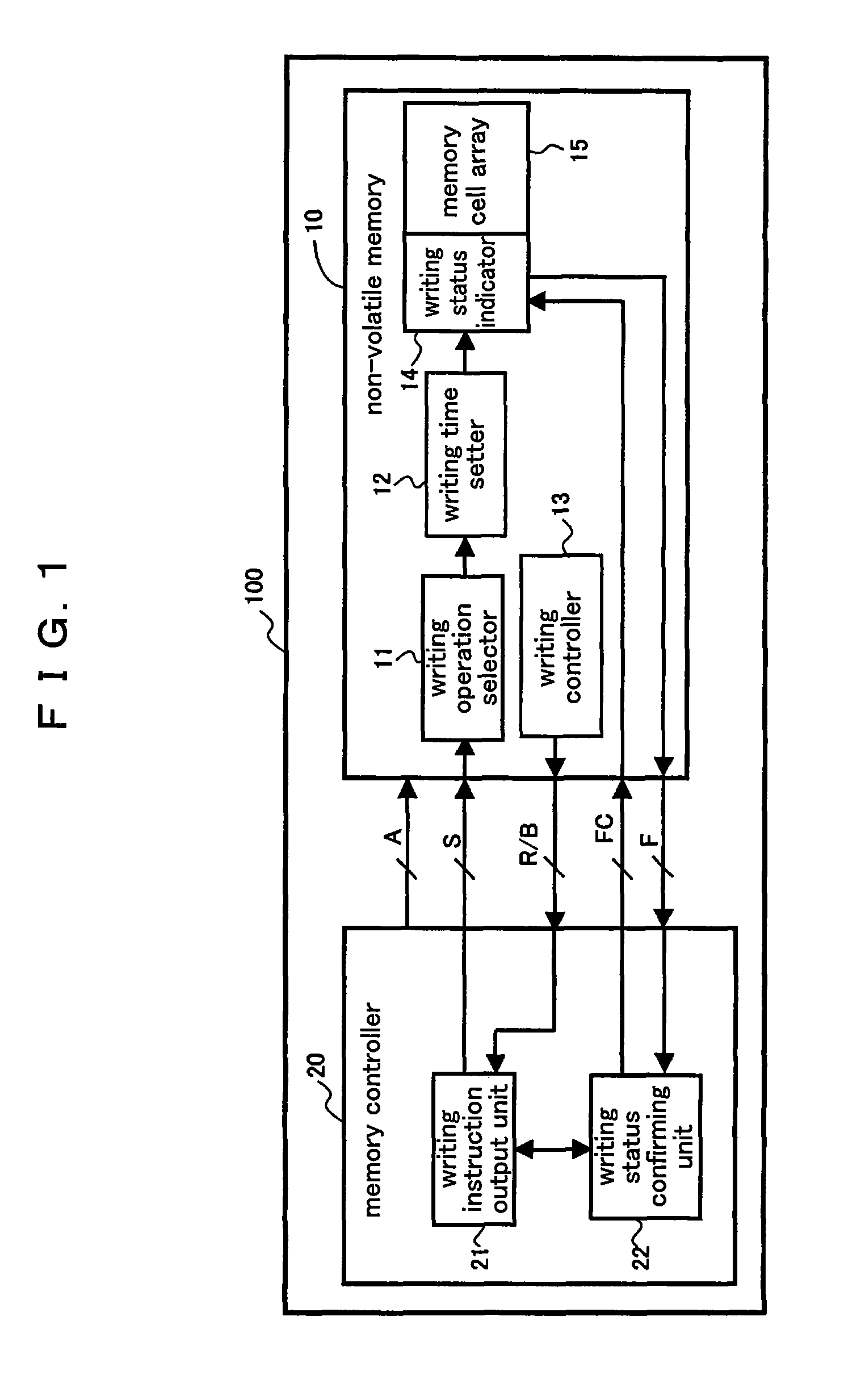
[0124]FIG. 2 is a block diagram illustrating a constitution of a non-volatile memory control device 100 according to a preferred embodiment 2 of the present invention. In FIG. 2, the same reference symbols as those shown in FIG. 1 (preferred embodiment 1) denote the same constituent elements. The non-volatile memory control device 100 according to the present preferred embodiment comprises m number of non-volatile memories 10 (m is an arbitrary natural number). It is assumed that there are n number (n is an arbitrary natural number which satisfies m>n) of non-volatile memories 10 to which the rejection of the writing operation is not outputted from the writing controller 13 for at least a certain period of time. In the assumed case, the writing instruction output unit 21 outputs the additional writing instruction to a non-volatile memory 10 arbitrarily selected, and thereafter outputs the temporary writing instruction to another non-volatile memory 10 by the ti...

embodiment 3

Preferred Embodiment 3

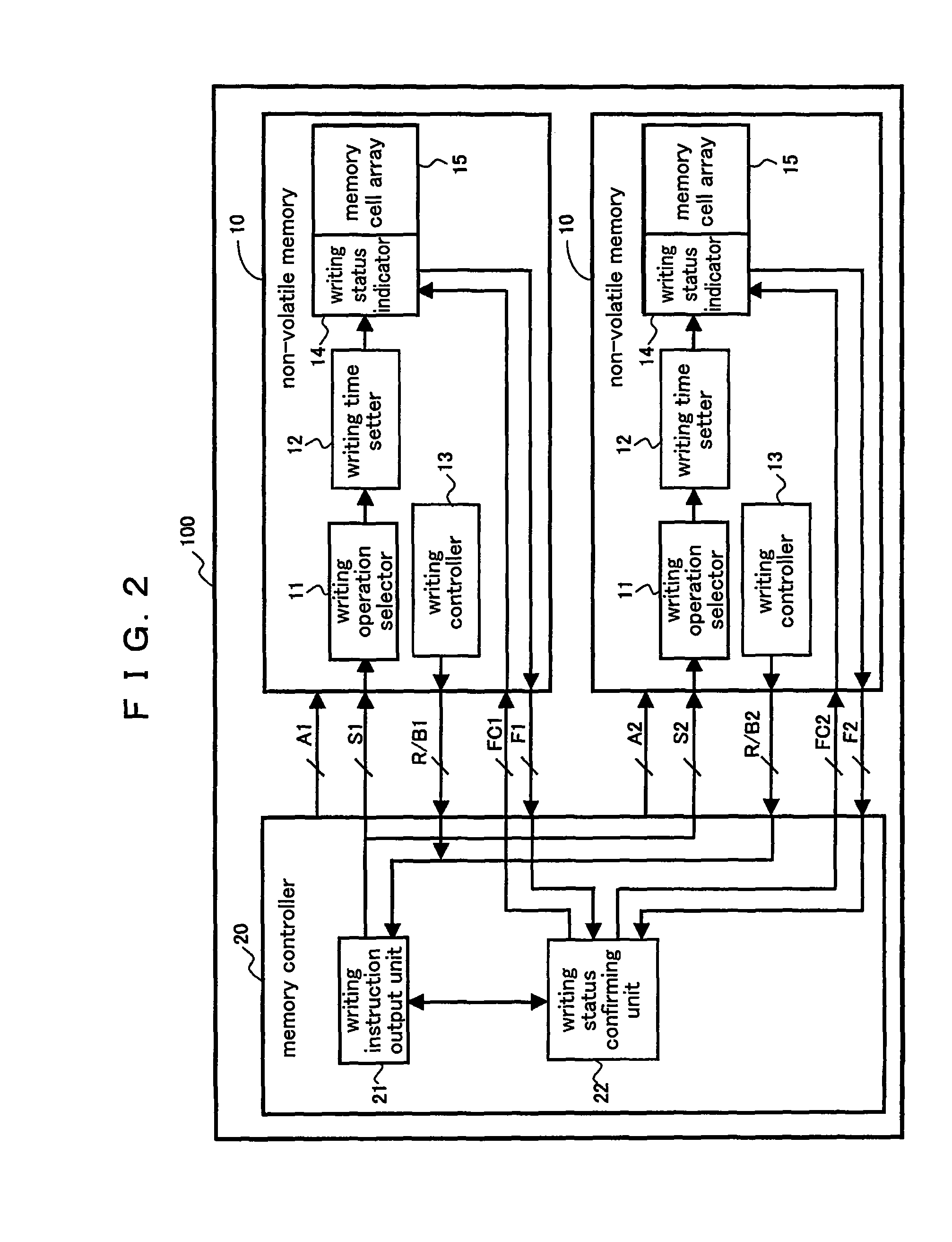
[0129]FIG. 4 is a block diagram illustrating a constitution of a non-volatile memory control device 100 according to a preferred embodiment 3 of the present invention. In FIG. 4, the same reference symbols as those shown in FIG. 2 (preferred embodiment 2) denote the same constituent elements. In the non-volatile memory control device 100 according to the present preferred embodiment, the memory controller 20 further comprises a power-on detector 23 for detecting the power-on of the device. The power-on detector 23 activates the writing status confirming unit 22 upon the detection of the power-on of the device. When the activated writing status confirming unit 22 identifies a memory block in which a temporary writing operation is completed but an additional writing operation is not executed yet, the power-on detector 23 activates the writing instruction output unit 21 so that the additional writing instruction is outputted therefrom.

[0130]It is assumed that the ...


PUM


Abstract

A memory controller outputs an additional writing instruction to one of a plurality of non-volatile memories arbitrarily selected via a writing instruction output unit when a signal which rejects a writing operation is not outputted from writing controllers of the plurality of non-volatile memories for a certain period of time, and outputs a temporary writing instruction to another non-volatile memory at least once via the writing instruction output unit by the time when the additional writing operation is completed in the arbitrary non-volatile memory.

Description

BACKGROUND OF THE INVENTION[0001]1. Field of the Invention[0002]The present invention relates to a device for controlling a non-volatile memory in which data can be electrically written and erased, more particularly to a technology for reducing an amount of time which is apparently necessary for writing data from a memory controller in the non-volatile memory.[0003]2. Description of the Related Art[0004]A conventional non-volatile memory control device, which is recited in the Japanese Patent Publication (No. 2004-253093 of the Japanese Patent Applications Laid-Open) is described referring to FIGS. 9-11C. FIG. 9 is a block diagram illustrating a constitution of a conventional EEPROM (Electrically Erasable Programmable Read Only Memory), FIG. 10A is a sectional view of a floating-gate memory cell transistor of the conventional EEPROM, FIG. 10B is an illustration of a constitution of a memory cell array, FIG. 11A is an illustration of a writing-time dependency of a writing-status thre...

Claims


Application Information

Patent Timeline
Patent Type & Authority Patents(United States)
IPC IPC(8): G11C11/34G11C16/04G11C7/00
CPCG06F13/16G11C16/10
Inventor MISUMI, KENJI
Owner CETUS TECH INC
Why Eureka
Eureka Blog
Learn More