Eureka AIR delivers breakthrough ideas for toughest innovation challenges, trusted by R&D personnel around the world.

Semiconductor integrated circuit

a technology of integrated circuits and semiconductors, applied in the direction of pulse techniques, solid-state devices, instruments, etc., can solve the problems of inability to recover logic portions that become defective in wafer processing, high manufacturing costs, and high cost of producing exposure masks. , to achieve the effect of high-speed memory access operations and shortened data write times between the separation portion and the memory cells

Active Publication Date: 2006-01-10
CETUS TECH INC
View PDF15 Cites 0 Cited by
  • Summary
  • Abstract
  • Description
  • Claims
  • Application Information

AI Technical Summary

Benefits of technology

[0007]In consideration of the above-described problems, it is an object of the present invention to make it possible for a semiconductor integrated circuit that includes an integration of a memory such as a DRAM and a logic portion such as a microprocessor or an ASIC, to be switched to the desired system LSI for a specific purpose, after it has undergone steps from development to wafer processing using the same exposure masks, and to improve productivity. Furthermore, it is an object to make it possible to recover a logic portion that has become defective in the wafer processing of a semiconductor integrated circuit, and to improve yield.

Problems solved by technology

However, with continuous shrinking of the manufacturing processes of semiconductor integrated circuits in recent years, producing exposure masks has become very expensive.
For this reason, producing separate exposure masks for each system LSI has increased manufacturing costs.
Furthermore, even though the DRAM in a conventional system LSI is prepared with redundant memory cells for substitution, the logic portion is not provided with redundant logic portions.
For this reason, a logic portion that becomes defective in wafer processing cannot be recovered, and semiconductor integrated circuits that have such a defective logic portion become defective products.
These kinds of reductions in yield also cause the cost of manufacturing semiconductor integrated circuits to increase.

Method used


Image

  • Semiconductor integrated circuit
  • Semiconductor integrated circuit
  • Semiconductor integrated circuit

Examples


first embodiment

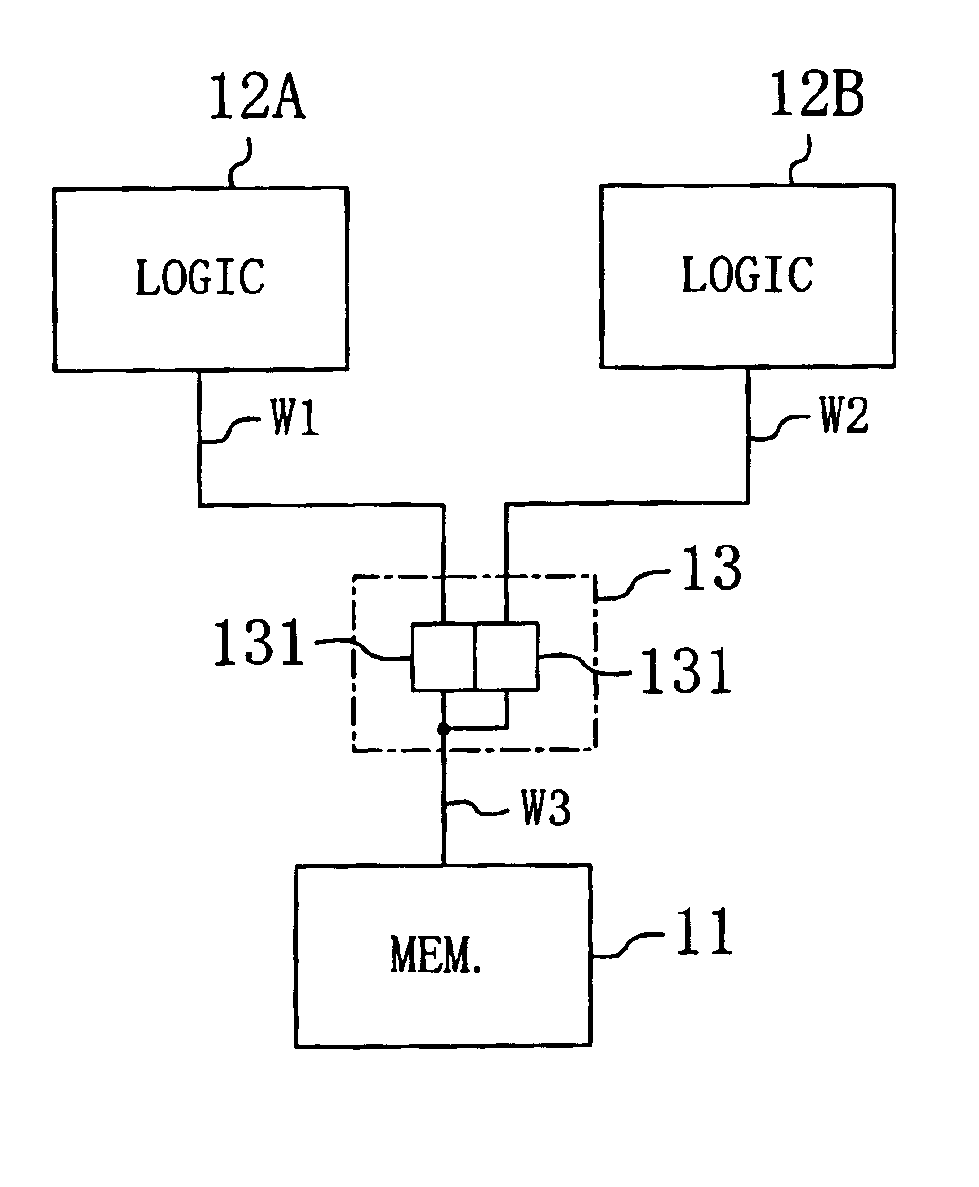
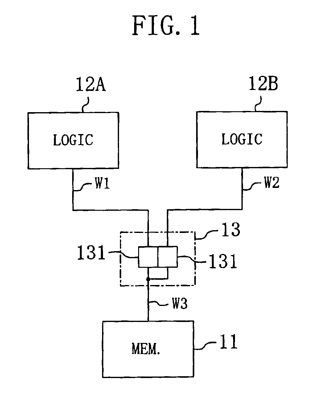
[0057]FIG. 1 shows a configuration of a semiconductor integrated circuit according to a first embodiment of the present invention. In this embodiment, the semiconductor integrated circuit includes: a memory 11, such as a DRAM (dynamic random access memory), an SRAM (static random access memory), a flash memory, a ROM (read only memory), or a ferroelectric memory; logic portions 12A and 12B that perform data processing, such as microprocessors, ASICs (application specific ICs) or the like; and a separation portion 13, integrated on a single substrate.

[0058]Although not shown in the drawing, the memory 11 and the logic portions 12A and 12B are respectively equipped with an address terminal, a data input terminal, a data output terminal, a data input / output terminal, and a clock terminal, for example. These terminals of the logic portions 12A and 12B are respectively connected to the separation portion 13 by wires W1 and W2, and each terminal of the memory 11 is also respectively conne...

second embodiment

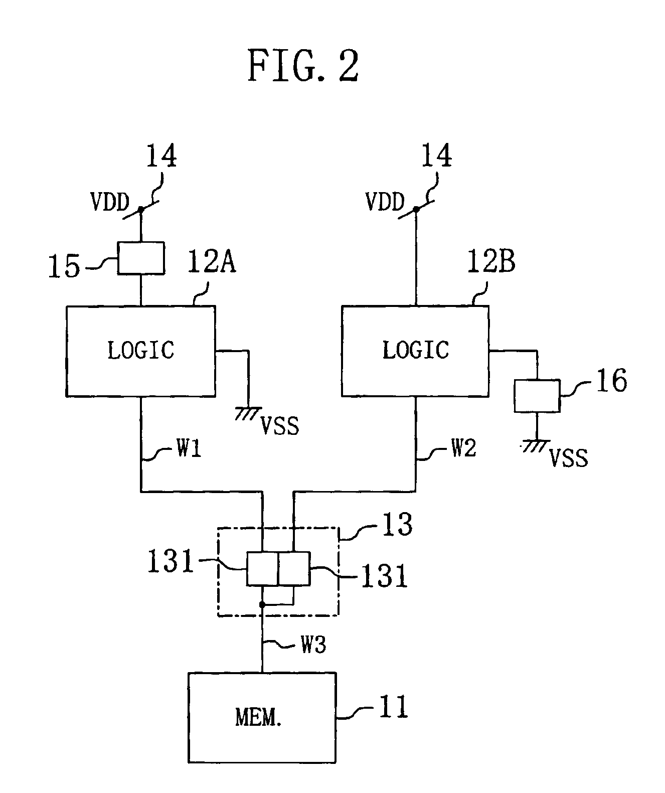
[0069]FIG. 2 shows a configuration of a semiconductor integrated circuit according to a second embodiment of the present invention. The semiconductor integrated circuit according to this embodiment is provided with, in addition to the semiconductor integrated circuit according to the first embodiment, a power source separation circuit 15 for separating a power source 14 that is supplied to the logic portion 12A, and a substrate voltage changing circuit 16 for changing a substrate voltage VSS of the logic portion 12B. The following is an explanation of aspects that differ from the first embodiment, particularly the operation of the power source separation cricuit 15 and the substrate voltage changing circuit 16.

[0070]The power source separation circuit 15 connects, or separates, the power source 14 and the logic portion 12A. Like the separation portion 13, it can be configured with fuses or antifuses, or switches such as MOS transistors.

[0071]The substrate voltage changing circuit 16...

third embodiment

[0076]FIG. 3 shows a configuration of a semiconductor integrated circuit according to a third embodiment of the present invention. In this embodiment, the semiconductor integrated circuit includes: a memory 11, a logic portion 12C that has a control circuit 121A, a logic portion 12D that has a control circuit 121B, and a separation portion 13A that has switching circuits for controlling the switching between connection and separation of the logic portions 12C / 12D and the memory 11, integrated on a single substrate.

[0077]As switching circuits, the separation portion 13A is provided with a plurality of (in this embodiment, two) transistor switches 132, arranged between the memory 11 and the logic portions 12C and 12D respectively. The transistor switches 132 are respectively allocated for every wire connecting each terminal of the logic portions 12C and 12D with each corresponding terminal of the memory 11.

[0078]The open / close operations of the transistor switches 132 are controlled b...


PUM


Abstract

A semiconductor integrated circuit with integrated memory and data-processing logic portions is provided, with which productivity and yield can be improved. The semiconductor integrated circuit is provided with a memory, a plurality of logic portions that are capable of being connected to the memory, and a separation portion that connects one of the plurality of logic portions to the memory, while separating the other logic portions from the memory. One required logic portion of the plurality of logic portions is connected to the memory, and the other non-required logic portions are separated from the memory, by the separation portion. The semiconductor integrated circuit can be switched for a system LSI after wafer processing, so this enables a plurality of system LSIs to be manufactured using the same exposure masks, thus improving productivity. Furthermore, defective logic portions can be recovered, thus improving the yield.

Description

BACKGROUND OF THE INVENTION[0001]The present invention relates to semiconductor integrated circuits, particularly the technology of semiconductor integrated circuits in which a memory and a data-processing logic portion are integrated.[0002]In recent years, DRAMs (dynamic random access memories) are increasingly made as macrocells, and there has been intensive integration of these with data-processing logic portions such as microprocessors and ASICs (application specific ICs), formed on a single semiconductor integrated circuit substrate. Semiconductor integrated circuits in which memory and logic portions are integrated in this way are called system LSIs.[0003]System LSIs are known for the following two advantages. First, there are the points that they eliminate restrictions originating in a DRAM's number of pins, they can expand the data width for data input / output, and they can dramatically improve the speed of data transfer between a DRAM and a logic portion. Second, there are t...

Claims


Application Information

Patent Timeline
Patent Type & Authority Patents(United States)
IPC IPC(8): G11C7/00G01R31/28G11C7/10G11C29/02G11C29/04H01L21/82H01L21/822H01L27/04H03K19/00
CPCG11C7/1006G11C2207/104
Inventor SHIBAYAMA, AKINORI
Owner CETUS TECH INC
Why Eureka
Eureka Blog
Learn More