Method of forming small pitch pattern using double spacers

a technology of double spacers and pattern patterns, which is applied in the direction of auxillary members of forms/shuttering/falseworks, instruments, photomechanical equipment, etc., can solve the problems of reducing design rules and pattern pitches, reducing pattern pitches, and challenging the resolution accuracy of conventional lithography equipment. resolution accuracy and resolution accuracy of conventional lithography equipment,

Active Publication Date: 2010-11-30
SAMSUNG ELECTRONICS CO LTD
View PDF19 Cites 41 Cited by
  • Summary
  • Abstract
  • Description
  • Claims
  • Application Information

AI Technical Summary

Problems solved by technology

As contemporary semiconductor devices increase in their constituent element densities, design rules for the layout of such elements have become increasingly small and very strict in their tolerances.
Such reduced design rules and reduced pattern pitches are beginning to challenge the resolution accuracy of conventional lithography equipment.
Alternatively, a lithography process using a F2 excimer laser having a shorter wavelength of 153 nm may ultimately be used, but this technique remains under development and has proved difficult to use in the formation patterns on a semiconductor substrate.
Such equipment is, without successful adaptation, ill-suited to the formation of smaller pitch patterns, such as those having a pitch of about 50 nm or less.

Method used


Image

  • Method of forming small pitch pattern using double spacers
  • Method of forming small pitch pattern using double spacers
  • Method of forming small pitch pattern using double spacers

Examples


Embodiment Construction

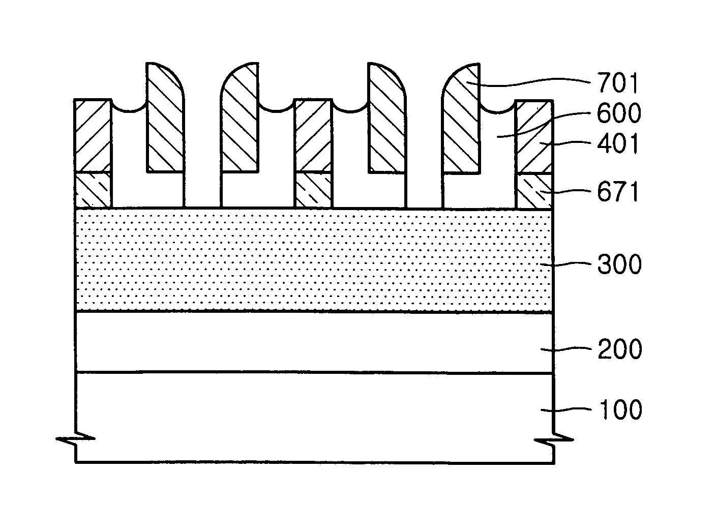
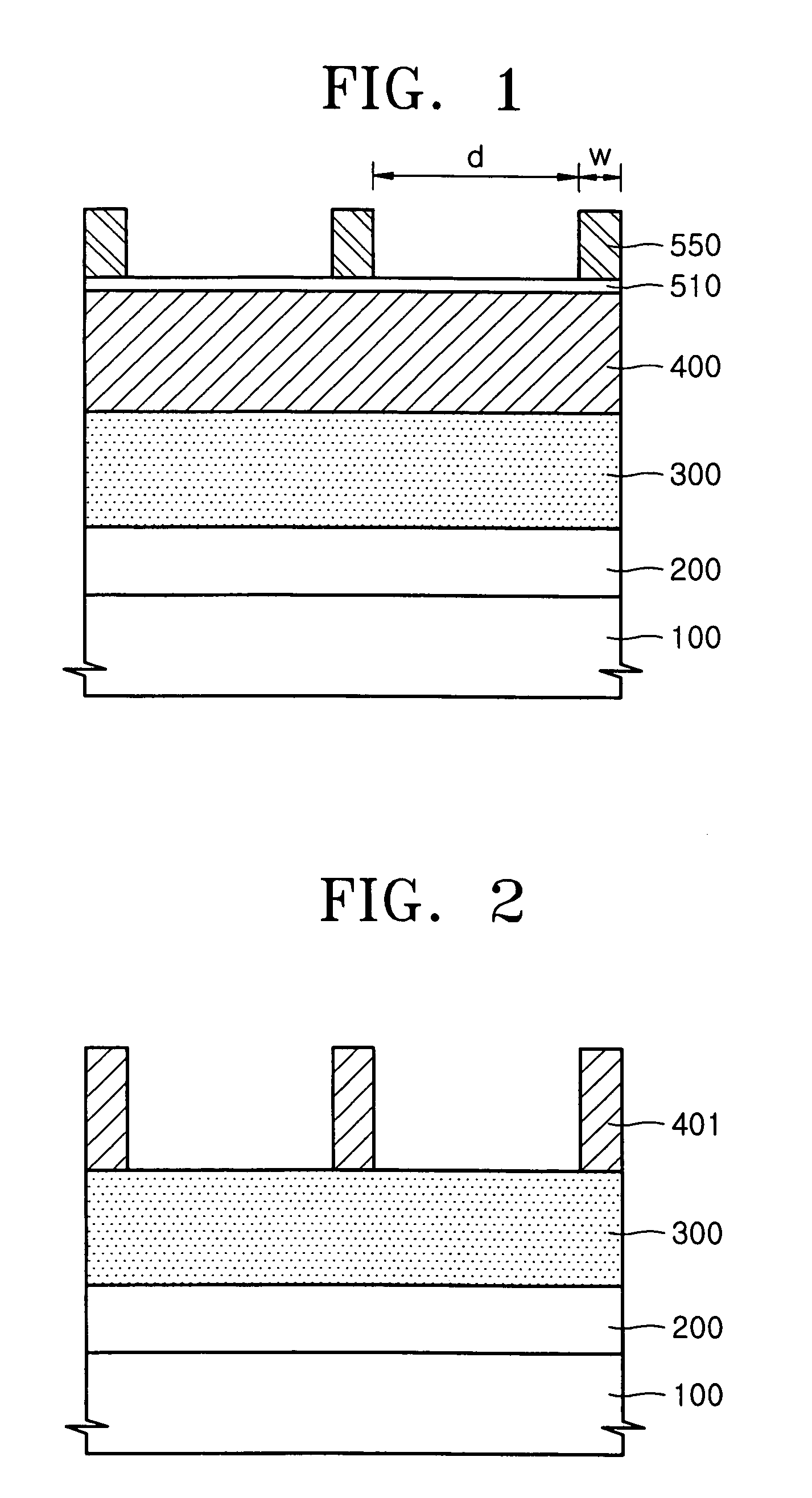
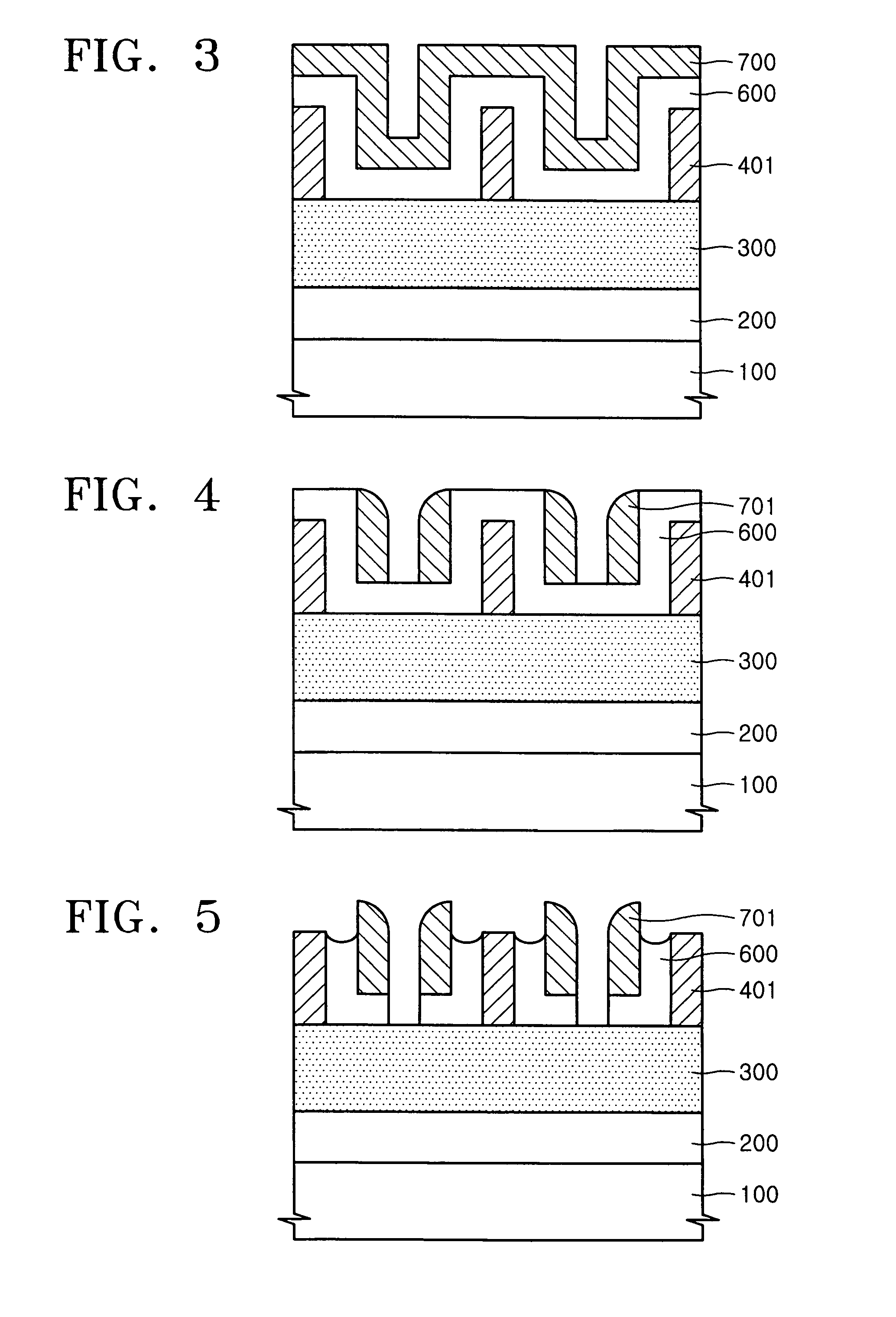
[0020]Several embodiments of the invention will now be described with reference to the accompanying drawings. The invention may, however, be embodied in many different forms and should not be construed as being limited to only the embodiments set forth herein. Rather, these embodiments are provided as teaching examples. Throughout this description and in the drawings like reference numbers refer to like or similar elements.

[0021]Embodiments of the invention provide a method for depositing double layers for double spacers on a small line pattern to cover the sidewall of the small line pattern, and performing a first spacer etch process on a second spacer layer to form a sidewall spacer. The double layers are deposited in such a manner that they extend to cover the sidewall of the small line pattern and to have a shape as if a spacer were attached in an axial direction.

[0022]An etch-back process or a spacer etch process is performed on the second spacer layer exposed by the first spac...


PUM


Abstract

A method of forming a small pitch pattern using double spacers is provided. A material layer and first hard masks are used and characterized by a line pattern having a smaller line width than a separation distance between adjacent mask elements. A first spacer layer covering sidewall portions of the first hard mask and a second spacer layer are formed, and spacer-etched, thereby forming a spacer pattern-shaped second hard mask on sidewall portions of the first hard mask. A portion of the first spacer layer between the first hard mask and the second hard mask is selectively removed. The material layer is selectively etched using the first and second hard masks as etch masks, thereby forming the small pitch pattern.

Description

BACKGROUND OF THE INVENTION[0001]1. Field of the Invention[0002]Embodiments of the invention relate to a semiconductor device fabrication method. More particularly, embodiments of the invention relate to a method of forming a small pitch pattern using double spacers.[0003]This application claims the benefit of Korean Patent Application No. 2005-0033205 filed on Apr. 21, 2005, the subject matter of which is hereby incorporated by reference in its entirety.[0004]2. Description of the Related Art[0005]The fabrication of a semiconductor device requires the application of multiple individual processes such as lithography, material deposition, patterning, etching, cleaning, etc. As contemporary semiconductor devices increase in their constituent element densities, design rules for the layout of such elements have become increasingly small and very strict in their tolerances. Reduced design rules result in increasingly small pitch definitions for patterns used, for example, in lithography ...

Claims


Application Information

Patent Timeline
Patent Type & Authority Patents(United States)
IPC IPC(8): H01L21/4763
CPCH01L21/0337H01L21/0338E04G17/0758
Inventor LEE, JI-YOUNGPARK, JOON-SOOWOO, SANG-GYUN
Owner SAMSUNG ELECTRONICS CO LTD
Why Eureka
Try Eureka