Non-streaming high-efficiency perforated semiconductor neutron detectors, methods of making same and measuring wand and detector modules utilizing same

a technology of perforated semiconductors and neutron detectors, applied in the direction of instruments, measurement with semiconductor devices, material analysis, etc., can solve the problems of fragile devices, low design reliability, and poor performance of devices, and achieve the effect of reliable design

Active Publication Date: 2010-12-21
KANSAS STATE UNIV RES FOUND
View PDF14 Cites 23 Cited by
  • Summary
  • Abstract
  • Description
  • Claims
  • Application Information

AI Technical Summary

Benefits of technology

[0057]An object of the present invention is to provide non-streaming high-efficiency perforated semiconductor neutron detectors, methods of making same and measuring wands and detector modules utilizing same, wherein in at least one embodiment of the invention sinuous channels such as chevron, sinusoidal, or circular channels are provided to correct the angular streaming problem while mechanically strengthening the semiconductor fins dividing the channels. Also, in at least one embodiment of the invention, a process is provided that reduces leakages currents while allowing for a straightforward method to backfill the perforations with neutron reactive materials such as 10B or 6LiF.
[0058]In carrying out the above object and other objects of the present invention, an apparatus is provided for efficiently detecting neutrons. The apparatus includes a particle-detecting first substrate having top and back surfaces and an array of sinuous fins spaced apart by a corresponding array of sinuous channels at the top surface. The apparatus further includes neutron-responsive material disposed in the array of sinuous channels. The material is responsive to neutrons absorbed thereby for releasing ionizing radiation reaction products wherein the sinuous shape of the fins and channels strengthens the fins and reduces neutron streaming effects whereby the apparatus has a relatively flat and uniform detection efficiency response.

Problems solved by technology

However, the circular hole and straight channel designs have problems that cause the devices to perform poorly at particular angles to neutron sources in which neutrons can “stream” through the device at lower detection efficiencies.
Further, the basic straight channel design leaves behind weak and easily broken fins of semiconductor material that separate the straight channels, hence the device is fragile.
Perforated structures built as described in previous works have severe leakage currents due to poor insulation between the perforations and the reverse biased diode junctions.
Finally, a method to fill the perforations, although demonstrated in previous works, has been elusive.

Method used


Image

  • Non-streaming high-efficiency perforated semiconductor neutron detectors, methods of making same and measuring wand and detector modules utilizing same
  • Non-streaming high-efficiency perforated semiconductor neutron detectors, methods of making same and measuring wand and detector modules utilizing same
  • Non-streaming high-efficiency perforated semiconductor neutron detectors, methods of making same and measuring wand and detector modules utilizing same

Examples


Embodiment Construction

)

Non-Streaming Perforated Detector Designs to Produce Relatively Uniform Response for Improved Detection Efficiency

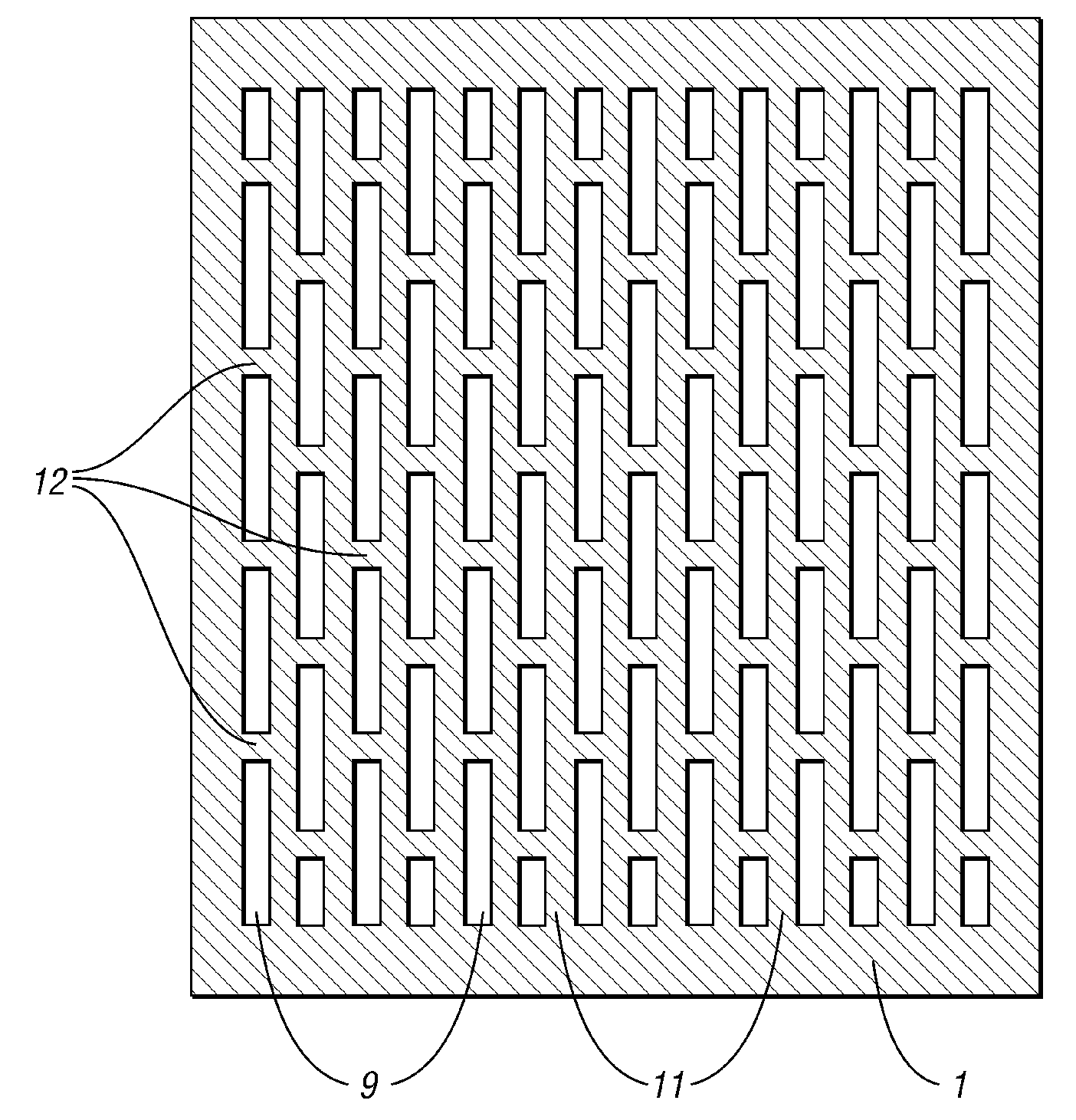
[0151]As previously mentioned, prior art perforated detectors where the neutrons have straight streaming paths do not offer desired angular efficiencies. Therefore, more complicated geometries are desired. Also, the fragility of prior art detectors having straight channels results in reduced detector yield.

[0152]Referring now to FIG. 23, to improve the strength of such channels, reinforcing links 12 were added into the design of FIGS. 3, 6, 7, 8, 9 and 21 wherein the same or similar components have the same reference number. When taking this to an extreme, the end result is an array of chevron-shaped perforations covering the semiconductor to both improve the neutron detection efficiency response and mechanically strengthen the structure. The first alternative geometry considered was a chevron (zig-zagged channel) pattern as shown in FIGS. 23a, 23b, 23c and 23d.

[0153]T...


PUM


Abstract

Non-streaming high-efficiency perforated semiconductor neutron detectors, method of making same and measuring wands and detector modules utilizing same are disclosed. The detectors have improved mechanical structure, flattened angular detector responses, and reduced leakage current. A plurality of such detectors can be assembled into imaging arrays, and can be used for neutron radiography, remote neutron sensing, cold neutron imaging, SNM monitoring, and various other applications.

Description

CROSS-REFERENCE TO RELATED APPLICATIONS[0001]This application claims the benefit of U.S. provisional application entitled “Non-Streaming Perforated Semiconductor Neutron Detector and Dosimeter and Method of Making the Same,” filed Mar. 16, 2006 and having Application U.S. Ser. No. 60 / 782,965.STATEMENT REGARDING FEDERALLY SPONSORED RESEARCH OR DEVELOPMENT[0002]This invention was made with Government support under DTRA contract DTRA-01-03-C-0051, National Science Foundation IMR-MIP Grant No. 0412208, and U.S. Department of Energy NEER Grant DE-FG07-041D14599. The United States Government has certain rights in this invention.BACKGROUND OF THE INVENTION[0003]1. Field of the Invention[0004]This invention generally relates to semiconductor radiation detectors and methods of making same and, in particular, to semiconductor detectors designed to detect neutrons of various energy ranges, methods of making same and measuring wands and detector modules utilizing such detectors.[0005]2. Backgro...

Claims


Application Information

Patent Timeline
Patent Type & Authority Patents(United States)
IPC IPC(8): G01T3/00
CPCG01T3/08
Inventor MCGREGOR, DOUGLAS S.SHULTIS, JOHN K.RICE, BLAKE B.MCNEIL, WALTER J.SOLOMON, CLELL J.PATTERSON, ERIC L.BELLINGER, STEVEN L.
Owner KANSAS STATE UNIV RES FOUND
Why Eureka
Try Eureka