Circuit and method using distributed phase change elements for across-chip temperature profiling

a phase change element and circuit technology, applied in the field of cross-chip temperature profiling, can solve the problems of significant area penalties, difficult integration into current state of the art technologies, and difficult connection voltage differences, and achieve the effect of greater sensing flexibility

Inactive Publication Date: 2011-02-01
GLOBALFOUNDRIES INC
View PDF20 Cites 7 Cited by
  • Summary
  • Abstract
  • Description
  • Claims
  • Application Information

AI Technical Summary

Benefits of technology

[0011]It should be noted that in order for the comparator circuit to function, as described, additional features may be required to eliminate or at least compensate for non-temperature related variations in voltages measured at the inputs to the sense amplifier. Such non-temperature related voltage differences can be caused by differences in amorphous resistances between the reference phase change element and the selected phase change element, due to process variations. Such non-temperature related voltage differences can also be caused by differences in parasitic wiring resistances, due to relative distances of the reference phase change element and the selected phase change element from the voltage difference detection device. Specifically, in order to compensate for these non-temperature related voltage differences, the comparator circuit can further comprise a third current source adapted to generate a third current (i.e., a sense leg bias current (ISense Bias)). This third current source can be electrically connected to a third node between the first node and the switching circuit in order to adjust the amorphous resistance of the selected phase change element to below a predetermined level. Additionally, in the case where the reference phase change element is a different selected one of the distributed phase change elements (as opposed to a permanently designated phase change element), a fourth current source can be electrically connected to a fourth node between the second node and the second switching current. This fourth current source can similarly generate a fourth current (i.e., a reference leg bias current (IRef Bias)) in order to adjust the amorphous resistance of the selected reference phase change element to below the predetermined level. Yet another technique used to avoid voltage differences at the input nodes of the sense amplifier (e.g., in the case where the reference phase change element is not permanently designated) is to ensure that the two switching circuits are adapted to select the phase change elements for sensing and reference from the same region of the semiconductor chip, thereby minimizing or avoiding all together differences in parasitic wiring resistances.
[0016]In this embodiment the third current source can be directly connected to the second node so that a pre-set current can supplied to the comparator circuit. Alternatively, the third current source can be connected to the second node via a current mirror circuit. This current mirror allows for selectable gain (i.e., the value of the third current (IRef2) can be multiplied, for example, by up to 100). This provides the comparator circuit with greater sensing flexibility.

Problems solved by technology

However, as integrated circuits continue to be scaled in size, the use of conventional analog temperature sensors can result in significant area penalties.
Additionally, such temperatures sensors often operate at relatively high operating voltages making their integration into current state of the art technologies, with relatively low operating voltages, more difficult.
Such non-temperature related voltage differences can also be caused by differences in parasitic wiring resistances, due to relative distances of the reference phase change element and the selected phase change element from the voltage difference detection device.

Method used


Image

  • Circuit and method using distributed phase change elements for across-chip temperature profiling
  • Circuit and method using distributed phase change elements for across-chip temperature profiling
  • Circuit and method using distributed phase change elements for across-chip temperature profiling

Examples


Embodiment Construction

[0024]The embodiments of the invention and the various features and advantageous details thereof are explained more fully with reference to the non-limiting embodiments that are illustrated in the accompanying drawings and detailed in the following description.

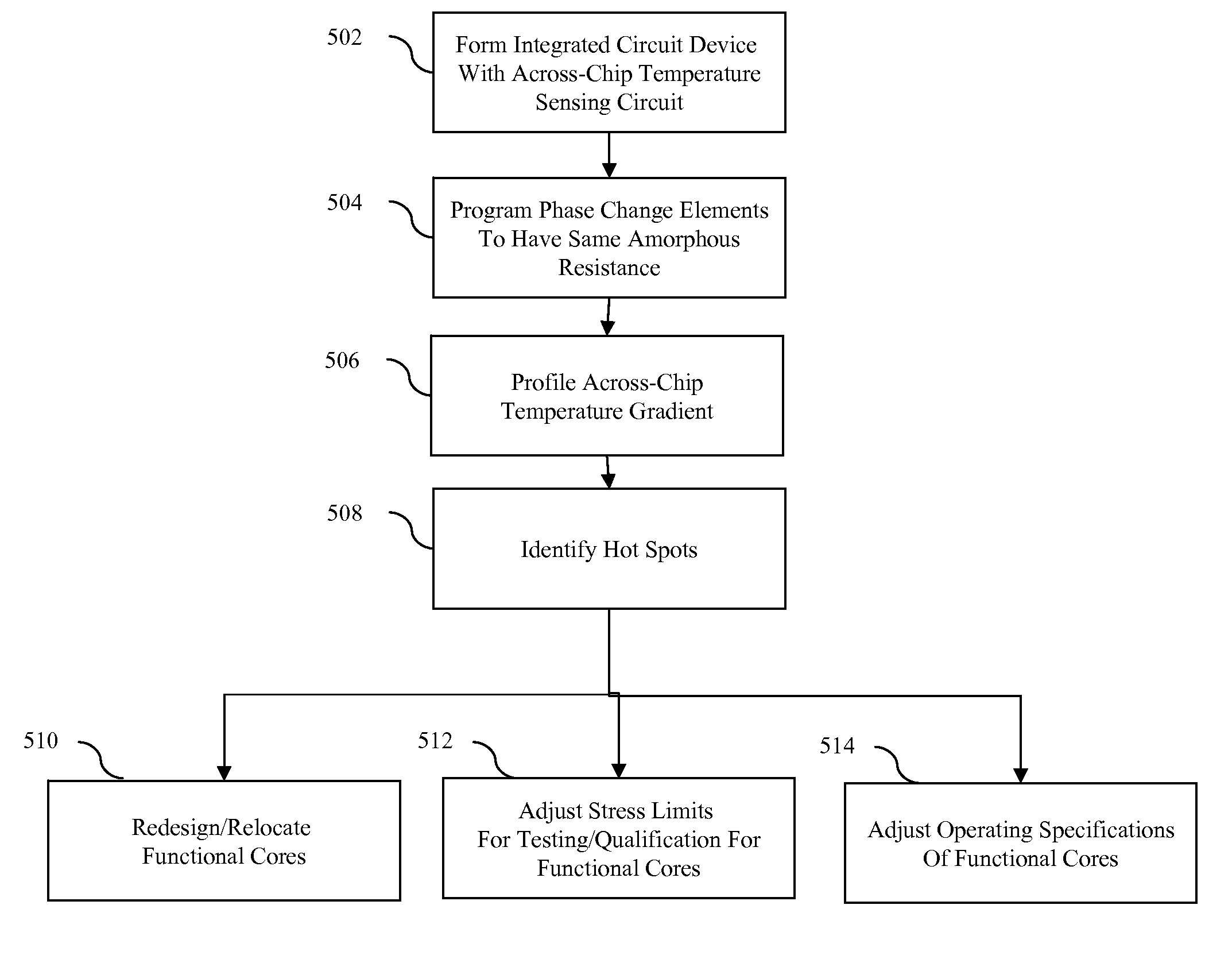
[0025]As mentioned above, operational performance of integrated circuit devices can be significantly affected by temperature variations, due to temperature-dependent characteristics, such as charge carrier mobility, threshold voltage, resistance, etc. Consequently, the temperature gradient across a semiconductor chip can be profiled to set up the needed stress levels for testing and qualification of system-on-chip (SOC) functional cores (e.g., third party intellectual property (IP) cores, logic cores, memory cores, processor cores, etc.) and further to set operational specifications (e.g., operating voltages) for SOC functional cores.

[0026]On-chip temperature sensors are useful tools for profiling temperature gradients. Howeve...


PUM


Abstract

Disclosed is an across-chip temperature sensing circuit and an associated method that can be used to profile the across-chip temperature gradient. The embodiments incorporate a plurality of phase change elements distributed approximately evenly across the semiconductor chip. These phase change elements are programmed to have essentially the same amorphous resistance. Temperature-dependent behavior exhibited by each of the phase change elements individually is compared to a reference (e.g., generated by a discrete reference phase change element, generated by another one of the phase change elements, or generated by an external reference) in order to profile the temperature gradient across the semiconductor chip. Once profiled, this temperature gradient can be used to redesign and / or relocate functional cores, to set stress limits for qualification of functional cores and / or to adjust operating specifications of functional cores.

Description

BACKGROUND[0001]1. Field of the Invention[0002]The embodiments of the invention generally relate to across-chip temperature profiling and, more particularly, to a circuit and a method that use distributed phase change memory (PCM) elements for across-chip temperature profiling.[0003]2. Description of the Related Art[0004]Operational performance of integrated circuit devices can be significantly affected by temperature variations, due to temperature-dependent characteristics, such as charge carrier mobility, threshold voltage, resistance, etc. Consequently, the temperature gradient across a semiconductor chip can be profiled to set up the needed stress levels for testing and qualification of system-on-chip (SOC) functional cores (e.g., third party intellectual property (IP) cores, logic cores, memory cores, processor cores, etc.) and further to set operational specifications (e.g., operating voltages) for SOC functional cores.[0005]On-chip temperature sensors are useful tools for pro...

Claims


Application Information

Patent Timeline
Patent Type & Authority Patents(United States)
IPC IPC(8): G06F17/50
CPCG01K3/14G01K7/006G01K7/425
Inventor HABIB, NAZMULLAMOREY, MARK C. H.MAFFITT, THOMAS M.MCMAHON, ROBERT
Owner GLOBALFOUNDRIES INC
Why Eureka
Try Eureka