Display panel
a display panel and display technology, applied in non-linear optics, instruments, optics, etc., can solve problems such as affecting display quality, and achieve the effect of improving display quality, aperture ratio and transmittance of a pixel
- Summary
- Abstract
- Description
- Claims
- Application Information
AI Technical Summary
Benefits of technology
Problems solved by technology
Method used
Image
Examples
first embodiment
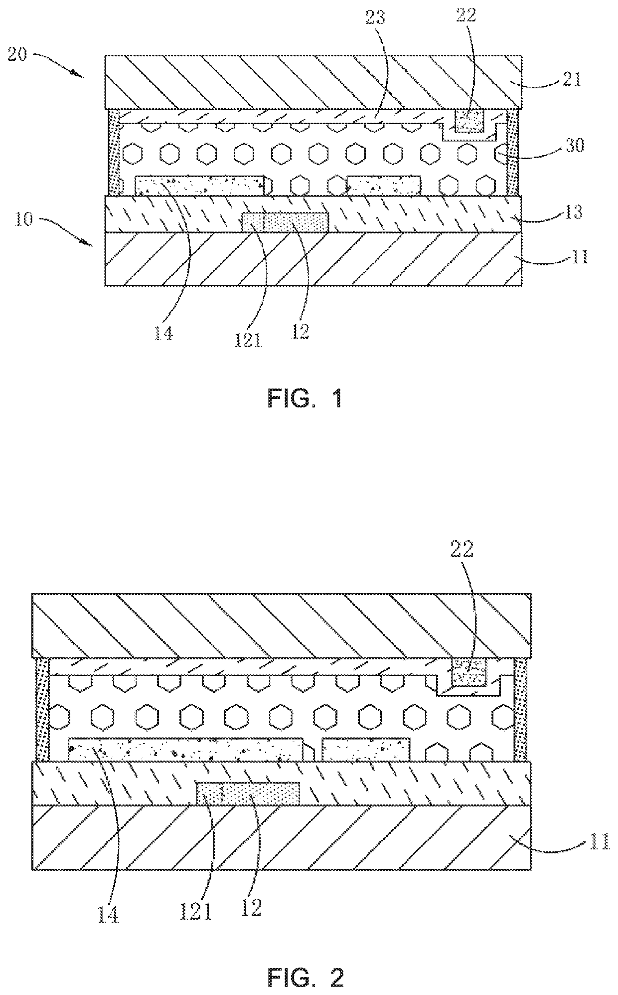
[0045]In a first embodiment, an orthographic projection of the black matrix 22 projected on the first substrate 11 does not coincide with an orthographic projection of the first edge portion 121 projected on the first substrate 11.
[0046]The pixel electrode 14 is used to shield the edge portion of the gate 12, so there is no need to provide the black matrix 22 directly above the edge portion of the gate 12. This reduces an area of the black matrix 22 and improves a pixel aperture ratio and transmittance.
second embodiment
[0047]In a second embodiment, as shown in FIG. 2, an orthographic projection of the pixel electrode 14 projected on the first substrate 11 covers an orthographic projection of the gate 12 projected on the first substrate 11.
[0048]Further, an orthographic projection of the black matrix 22 projected on the first substrate 11 does not coincide with the orthographic projection of the gate 12 projected on the first substrate 11. An area of the black matrix 22 is further reduced to improve the pixel aperture ratio and transmittance.
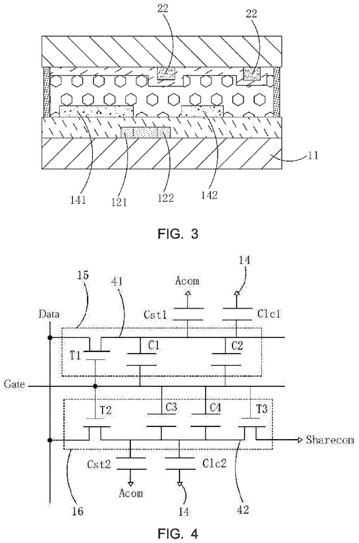
[0049]As shown in FIG. 3, the pixel electrode 14 comprises a main pixel electrode 141 and a sub-pixel electrode 142 that are independent of each other. The pixel unit has a primary region 15 and a secondary region 16. The primary pixel electrode 141 is disposed in the primary region 15, and the secondary pixel electrode 142 is disposed in the secondary region 16.
[0050]Wherein, the primary region 15 and the secondary region 16 may each comprise at least four dom...
third embodiment
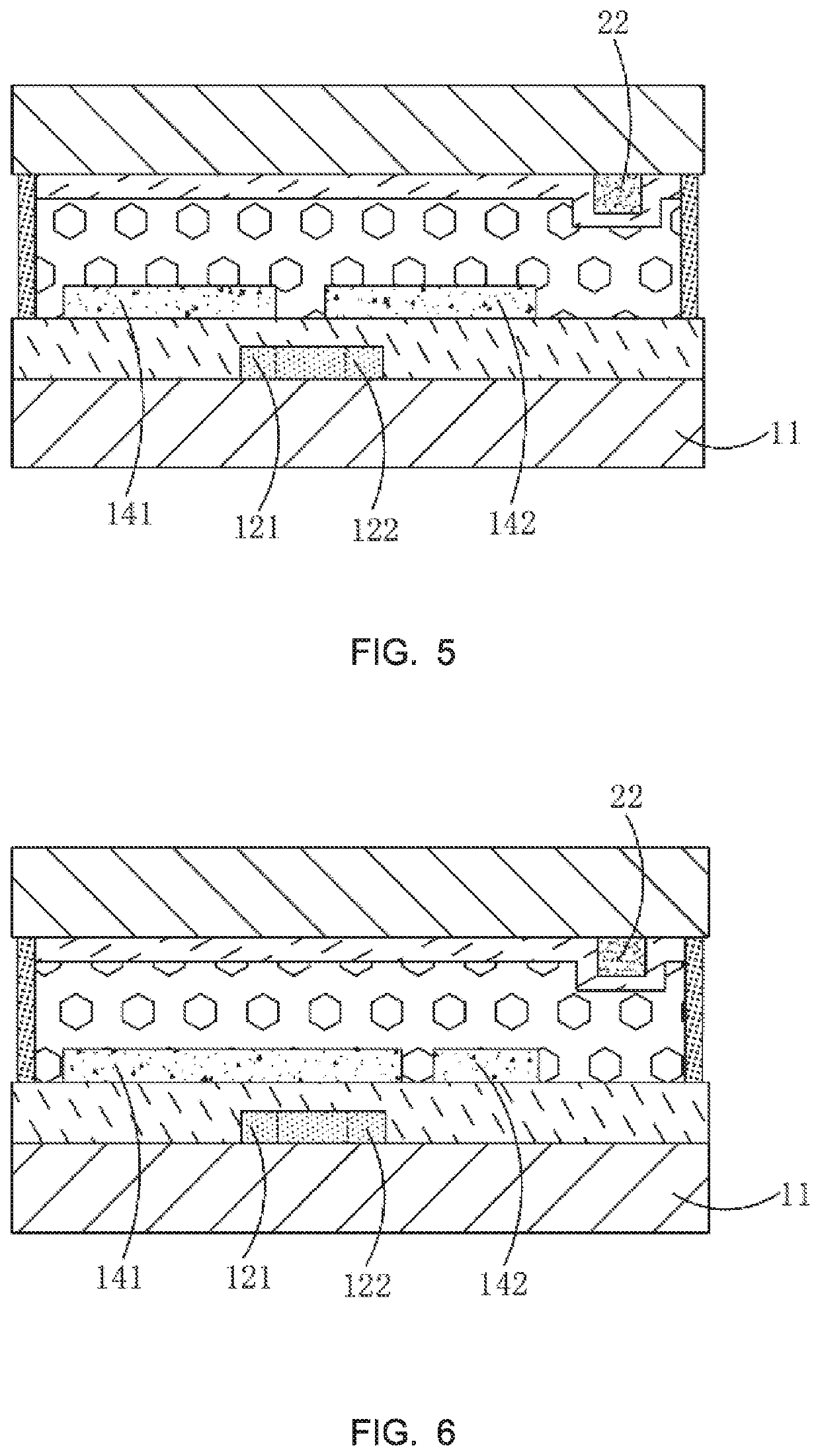
[0060]In a third embodiment, an orthographic projection of the sub-pixel electrode 142 projected on the first substrate 11 does not coincide with an orthographic projection of the gate 12 projected on the first substrate 11.
[0061]Further, an orthographic projection of the black matrix 22 projected on the first substrate 11 covers an orthographic projection of the second edge portion 122 projected on the first substrate 11.
[0062]Preventing a capacitance formed between the sub-pixel electrode 142 and the gate 12 from increasing the parasitic capacitance of the secondary region 16 causes the best common voltage of the primary region 15 and the best common voltage of the secondary region 16 to be different. Moreover, the main pixel electrode 141 and the black matrix 22 are used to block light on both sides of the gate 12 to prevent light leakage.
PUM
| Property | Measurement | Unit |
|---|---|---|
| voltage | aaaaa | aaaaa |
| electric field | aaaaa | aaaaa |
| transmittance | aaaaa | aaaaa |
Abstract
Description
Claims
Application Information


