Systems, methods, and apparatus for total coverage analysis and ranking of circuit designs

a total coverage analysis and circuit design technology, applied in the field of functional verification of circuit designs, can solve the problems of high manufacturing cost and complex current integrated circuit design

Active Publication Date: 2011-02-08
CADENCE DESIGN SYST INC
View PDF11 Cites 14 Cited by
  • Summary
  • Abstract
  • Description
  • Claims
  • Application Information

AI Technical Summary

Problems solved by technology

Current integrated circuit designs may be very complex and expensive to manufacture.

Method used


Image

  • Systems, methods, and apparatus for total coverage analysis and ranking of circuit designs
  • Systems, methods, and apparatus for total coverage analysis and ranking of circuit designs
  • Systems, methods, and apparatus for total coverage analysis and ranking of circuit designs

Examples


Embodiment Construction

[0018]In the following detailed description of the embodiments of the invention, numerous specific details are set forth in order to provide a thorough understanding of the present invention. However, it will be obvious to one skilled in the art that the embodiments of the invention may be practiced without these specific details. In other instances well known methods, procedures, components, and circuits have not been described in detail so as not to unnecessarily obscure aspects of the embodiments of the invention.

Introduction

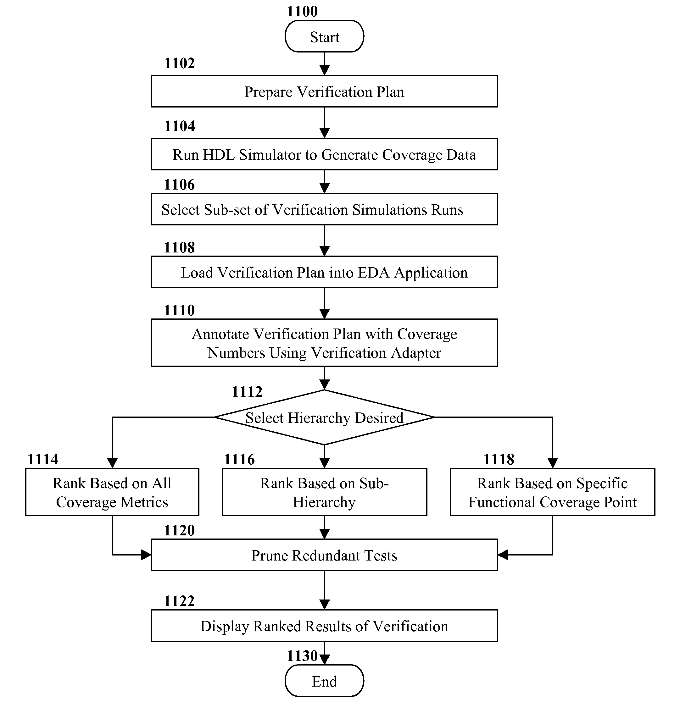
[0019]Coverage Driven Verification (CDV) is used by verification engineers to measure progress and completeness of verification of a circuit design. Since verification of complex system on chips (SOCs) has become enormously time-consuming and difficult to manage, verification engineers are gradually shifting towards a plan-based CDV methodology. The plan in this methodology refers to a verification plan used for tracking coverage obtained from various aspects...


PUM


Abstract

In some embodiments of the invention, a method and apparatus of consolidating all types of coverage metrics, obtained from an HDL simulator, under a single common framework is described. In other embodiments of the invention, a method and an apparatus are disclosed for performing ranking from a verification plan using total coverage metric.

Description

CROSS REFERENCE TO RELATED APPLICATIONS[0001]The instant application claims priority under 35 U.S.C. §119 to commonly assigned U.S. Provisional Patent Application Ser. No. 60 / 869,722, filed on Dec. 12, 2006, titled Methods and Apparatus for Total Coverage Analysis and Ranking of Circuit Designs, which is expressly incorporated herein in its entirety by this reference.FIELD[0002]The embodiments of the invention relate generally to functional verification of circuit designs. More particularly, the embodiments of the invention relate to coverage driven verification of integrated circuit designs.BACKGROUND[0003]Current integrated circuit designs may be very complex and expensive to manufacture. Thus, it is important that the functional design of an integrated circuit is verified prior to manufacturing.BRIEF SUMMARY[0004]The embodiments of the invention are summarized by the claims that follow below.BRIEF DESCRIPTIONS OF THE DRAWINGS[0005]FIG. 1A is an exemplary verification plan for a d...

Claims


Application Information

Patent Timeline
Patent Type & Authority Patents(United States)
IPC IPC(8): G06F17/50
CPCG01R31/318307G01R31/318314G01R31/318357G06F17/5081G06F30/398
Inventor CHAKRABORTI, SWAPNAJITPAGEY, SANDEEPGOMMERSHTADT, BORISDUEK-GOLAN, YAEL
Owner CADENCE DESIGN SYST INC
Why Eureka
Try Eureka