Method for fabricating P-channel field-effect transistor (FET)

a field-effect transistor and field-effect technology, applied in the field of integrated circuit fabrication methods, can solve the problems of increasing the size of the transistor, reducing the application range of conventional techniques, and reducing the effect of the short-channel

Active Publication Date: 2011-02-15
MARLIN SEMICON LTD
View PDF12 Cites 3 Cited by
  • Summary
  • Abstract
  • Description
  • Claims
  • Application Information

AI Technical Summary

Benefits of technology

[0011]The present invention is to provide a fabrication method of a semiconductor device, wherein the short-channel effects, caused by the size reduction of a device and an epitaxy growth process, can be mitigated.
[0017]According to an embodiment of the above fabrication method of a p-type channel field-effect transistor of the present invention, the implantation energy of the second co-implantation process is higher than that of the first co-implantation process.

Problems solved by technology

However, as the size of a transistor is further reduced, various problems generated from the short-channel effects become significant.
However, after the arrival of the 65 and 45 nm generations, the conventional technique is no longer applicable.
Ultimately, high electric field is resulted that in turns induces serious current leakage, especially at the side-wall-gate.
However, co-implantation with fluorine ions provides limited improvement on the saturation voltage.
Hence, it is ineffective in improving the short-channel effects.
Since the traveling speed of electrons and holes in a silicon channel is limited, the application of this approach in transistors is also limited.
However, during the formation of silicon germanium, the epitaxy growth process is conducted at extremely high temperature.
The heat provided for the formation of silicon germanium also causes the diffusion of boron, which ultimately leads to the short-channel effects.

Method used


Image

  • Method for fabricating P-channel field-effect transistor (FET)
  • Method for fabricating P-channel field-effect transistor (FET)
  • Method for fabricating P-channel field-effect transistor (FET)

Examples


Embodiment Construction

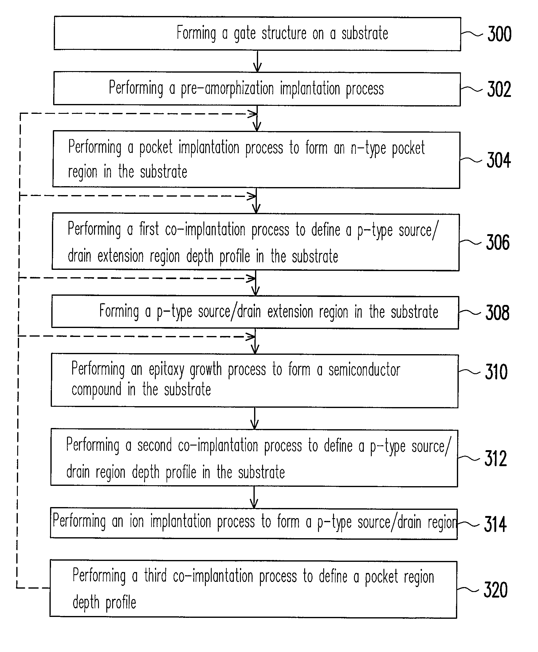
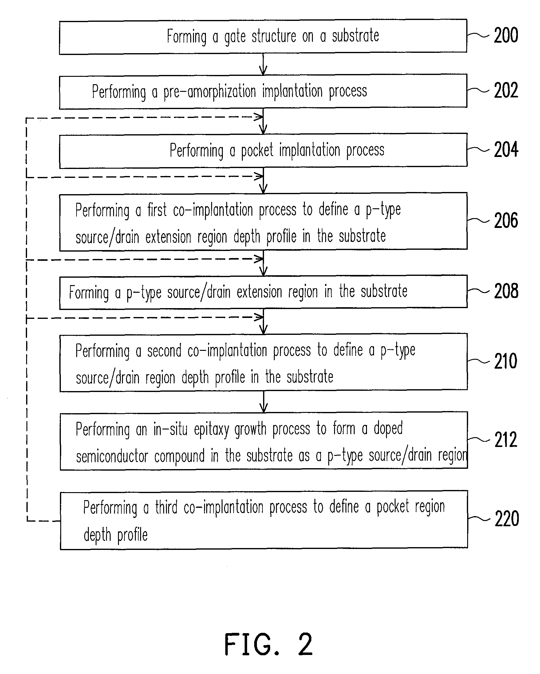
[0054]According to the fabrication method of a semiconductor device of the present invention, preceding the implantation process for the formation of, for example, the source / drain extension region of a p-type channel field-effect (FET) transistor or the source / drain region, or the pocket region of a p-type channel field-effect transistor (FET) wherein the species in the ion implantation process, such as the boron ion implantation, are susceptible to diffusion or generation of the short-channel effects, a co-implanation process is performed to lower the transient enhanced diffusion effect of boron ions and the formation of boron cluster. Further, another co-implantation process is performed before or after performing the pocket implantation process of a p-type FET to improve the effectiveness of the device.

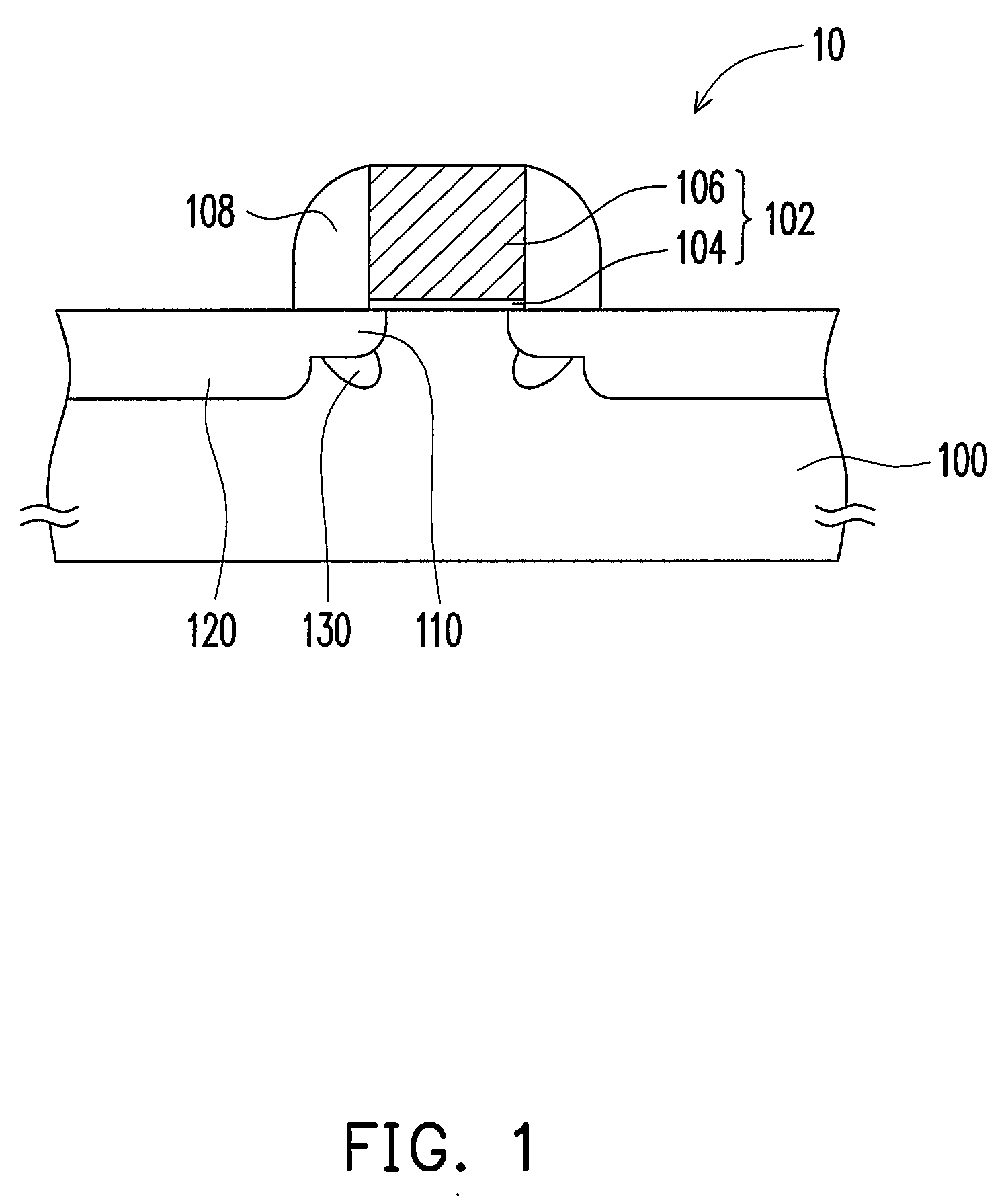
[0055]FIG. 1 is a schematic, cross-sectional view of a metal oxide semiconductor device. In one embodiment, the metal oxide semiconductor device formed on the substrate 100 is a P...


PUM


Abstract

A method for fabrication a p-type channel FET includes forming a gate on a substrate. Then, a PAI ion implantation process is performed. Further, a pocket implantation process is conducted to form a pocket region. Thereafter, a first co-implantation process is performed to define a source / drain extension region depth profile. Then, a p-type source / drain extension region is formed. Afterwards, a second co-implantation process is performed to define a source / drain region depth profile. Thereafter, an in-situ doped epitaxy growth process is performed to form a doped semiconductor compound for serving as a p-type source / drain region.

Description

BACKGROUND OF THE INVENTION[0001]1. Field of Invention[0002]The present invention relates to a fabrication method of integrated circuits. More particularly, the present invention relates to a fabrication method of a p-type channel field-effect transistor (FET).[0003]2. Description of Related Art[0004]The demand for high speed and low power consumption for logic devices can be accomplished by miniaturizing transistors. Scaling transistors to smaller dimensions can provide the logic devices with sufficiently high transistor saturation drain current and low gate capacitance for high speed and reduce leakage current for low power consumption.[0005]However, as the size of a transistor is further reduced, various problems generated from the short-channel effects become significant. The ultra-shallow junction formation technique is one method used to resolve the short-channel effects. According to the traditional ultra-shallow junction formation technique, after the formation of a gate ele...

Claims


Application Information

Patent Timeline
Patent Type & Authority Patents(United States)
IPC IPC(8): H01L21/336
CPCH01L21/26506H01L21/26513H01L21/26586H01L29/1083H01L29/6659H01L29/7833H01L21/26566H01L21/2658
Inventor LEE, KUN-HSIENHUANG, CHENG-TUNGHUNG, WEN-HANTING, SHYH-FANNJENG, LI-SHIANWU, MENG-YICHENG, TZYY-MING
Owner MARLIN SEMICON LTD
Why Eureka
Try Eureka