Pixel unit of high-speed cmos image sensor and manufacturing method thereof

An image sensor and pixel unit technology, applied in radiation control devices, etc., can solve problems such as low ion implantation energy, difficult transfer of photogenerated charges in photosensitive diodes, and influence of transfer transistor channel charge transfer, so as to reduce leakage and optimize process parameters , Eliminate the effect of afterimage

Active Publication Date: 2014-10-15
INST OF SEMICONDUCTORS - CHINESE ACAD OF SCI
View PDF5 Cites 0 Cited by
  • Summary
  • Abstract
  • Description
  • Claims
  • Application Information

AI Technical Summary

Problems solved by technology

[0008] figure 1 and figure 2 For the photosensitive diode, when the size of the photosensitive diode increases, it is difficult to form a CMOS image sensor without afterimage by adjusting the process parameters and device structure. transfer
[0009] figure 1 The ion implantation energy of the anti-punching region 105 is small, so the anti-punching region 105 is not deep enough, resulting in the risk of leakage current under the heavily doped region (also the floating diffusion region FD) 112 of the transfer transistor drain; and figure 2 The structure in which the doped well 309 is located under the heavily doped region of the drain of the transfer transistor affects the charge transfer in the channel of the transfer transistor because the doped well is close to the channel below the gate of the transfer transistor

Method used


Image

  • Pixel unit of high-speed cmos image sensor and manufacturing method thereof
  • Pixel unit of high-speed cmos image sensor and manufacturing method thereof
  • Pixel unit of high-speed cmos image sensor and manufacturing method thereof

Examples


Embodiment Construction

[0039] In order to make the object, technical solution and advantages of the present invention clearer, the present invention will be described in further detail below in conjunction with specific embodiments and with reference to the accompanying drawings.

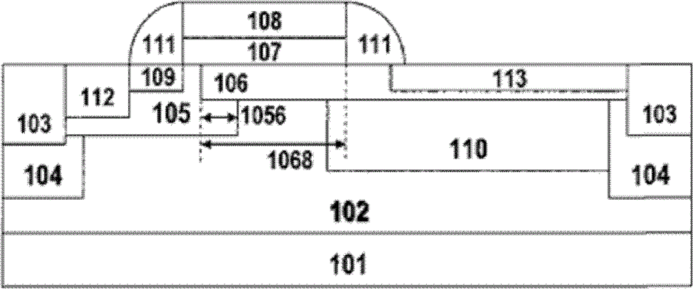
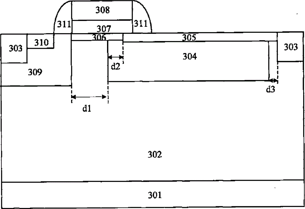
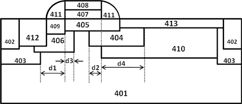
[0040] In the photosensitive diode of the pixel unit of the high-speed CMOS image sensor made in the prior art, it is difficult to transfer the photogenerated charge to the floating diffusion region FD completely quickly; Leakage of the small floating diffusion FD. Therefore, the present invention provides a pixel unit of a high-speed CMOS image sensor and a manufacturing method thereof, which improves the transfer speed of the photo-generated charge of the photosensitive diode; at the same time, by optimizing the position and The process parameters can significantly reduce the leakage of the FD without affecting the charge transfer of the transfer transistor channel.

[0041] In the embodiment of the present invention, ...


PUM


Abstract

The invention discloses a pixel unit of a high-speed CMOS (complementary metal oxide semiconductor) image sensor and a manufacturing method of pixel unit. The pixel unit comprises a monocrystalline silicon substrate, a shallow trench isolation region positioned in the monocrystalline silicon substrate and a doping well completely covering the lower part of the shallow trench isolation region, as well as a transfer transistor and a buried light-sensitive diode, wherein the transfer transistor and the buried light-sensitive diode are arranged in the shallow trench isolation region. According to the pixel unit disclosed by the invention, the transfer speed of photogenerated charges of the light-sensitive diode can be increased; and simultaneously, by optimizing the positions and the process parameters of an anti-reach through region and the doping well arranged on one side of a drain of the transfer transistor, the purpose of preventing the FD (field desorption) electric leakage can be achieved under the situation of no influence to the charge transfer in a trench below a gate of the transfer transistor.

Description

technical field [0001] The present invention relates to the technical field of Complementary Metal-Oxide-Semiconductor (CMOS for short), in particular to a pixel unit of a high-speed CMOS image sensor and a manufacturing method thereof. Background technique [0002] Image sensors are usually used to convert optical signals into electrical signals, and are an important part of digital cameras. According to different devices, they can be divided into charge coupled device (CCD for short) and CMOS image sensor (CMOS Image Sensor, referred to as CIS) two categories. Due to the broad application prospects of high-speed image sensors, such as automobile collision detection, high-speed scanning, machine vision and scientific research, etc., which require high frame rate image acquisition, in recent years, high-speed image sensors have developed rapidly. Compared with traditional CCD image sensors , CMOS image sensor has become the preferred technology for high-speed image sensor b...

Claims


Application Information

Patent Timeline
Patent Type & Authority Patents(China)
IPC IPC(8): H01L27/146
Inventor 曹中祥吴南健周杨帆李全良秦琦
Owner INST OF SEMICONDUCTORS - CHINESE ACAD OF SCI
Why Eureka
Try Eureka