Solid state imaging device and method of manufacturing the same

a solid-state imaging and imaging device technology, applied in the direction of semiconductor devices, radio frequency controlled devices, electrical devices, etc., can solve the problems of insufficient speed enhancement of transfer frequency, inability to uniform output of solid-state imaging devices, and reduced opening width, so as to achieve high sensitivity and reduce smearing

Active Publication Date: 2011-03-15
PANASONIC SEMICON SOLUTIONS CO LTD
View PDF6 Cites 0 Cited by
  • Summary
  • Abstract
  • Description
  • Claims
  • Application Information

AI Technical Summary

Benefits of technology

[0014]Therefore, with the foregoing in mind, it is an object of the present invention to provide a solid state imaging device that has a shunt wiring structure that solves the above-mentioned problem and that can perform a high-speed transfer at a high sensitivity and with reduced smearing, and to provide a method of manufacturing the solid state imaging device.
[0017]According to the thus configured solid state imaging device of the present invention, a voltage is fed to the second transfer electrode from the light-shielding film having isolation regions extending in the horizontal direction. Namely, as the light-shielding film is used as a shunt wiring, the wiring width can be increased sufficiently. Thereby, a high-speed transfer frequency can be obtained.
[0018]Furthermore, since there is no necessity to dispose a plurality of wirings on the first transfer electrodes, the width of the first transfer electrodes can be decreased at portions between the photodetector parts. Thereby, the opening width can be increased and a high sensitivity can be achieved.
[0019]Further, the light-shielding film isolated horizontally and the second transfer electrodes are connected electrically, and they have the same potential constantly. Thereby, at any time reading out a charge from the photodetector parts to the vertical transfer parts, readout pulses are applied also to the light-shielding film. Thus the width in the vertical transfer direction of the second transfer electrodes can be decreased in comparison with a case where the readout pulse is not applied to the light-shielding film. Therefore, the opening width can be increased, the sensitivity can be improved and smearing can be reduced.

Problems solved by technology

This will cause output nonuniformity for the solid state imaging device.
This will result in a problem that the speed of transfer frequency cannot be enhanced sufficiently even by using low-resistance shunt wirings.
This will result in another problem that the opening width is decreased and the smear property and the sensitivity deteriorate.

Method used


Image

  • Solid state imaging device and method of manufacturing the same
  • Solid state imaging device and method of manufacturing the same
  • Solid state imaging device and method of manufacturing the same

Examples


embodiment 1

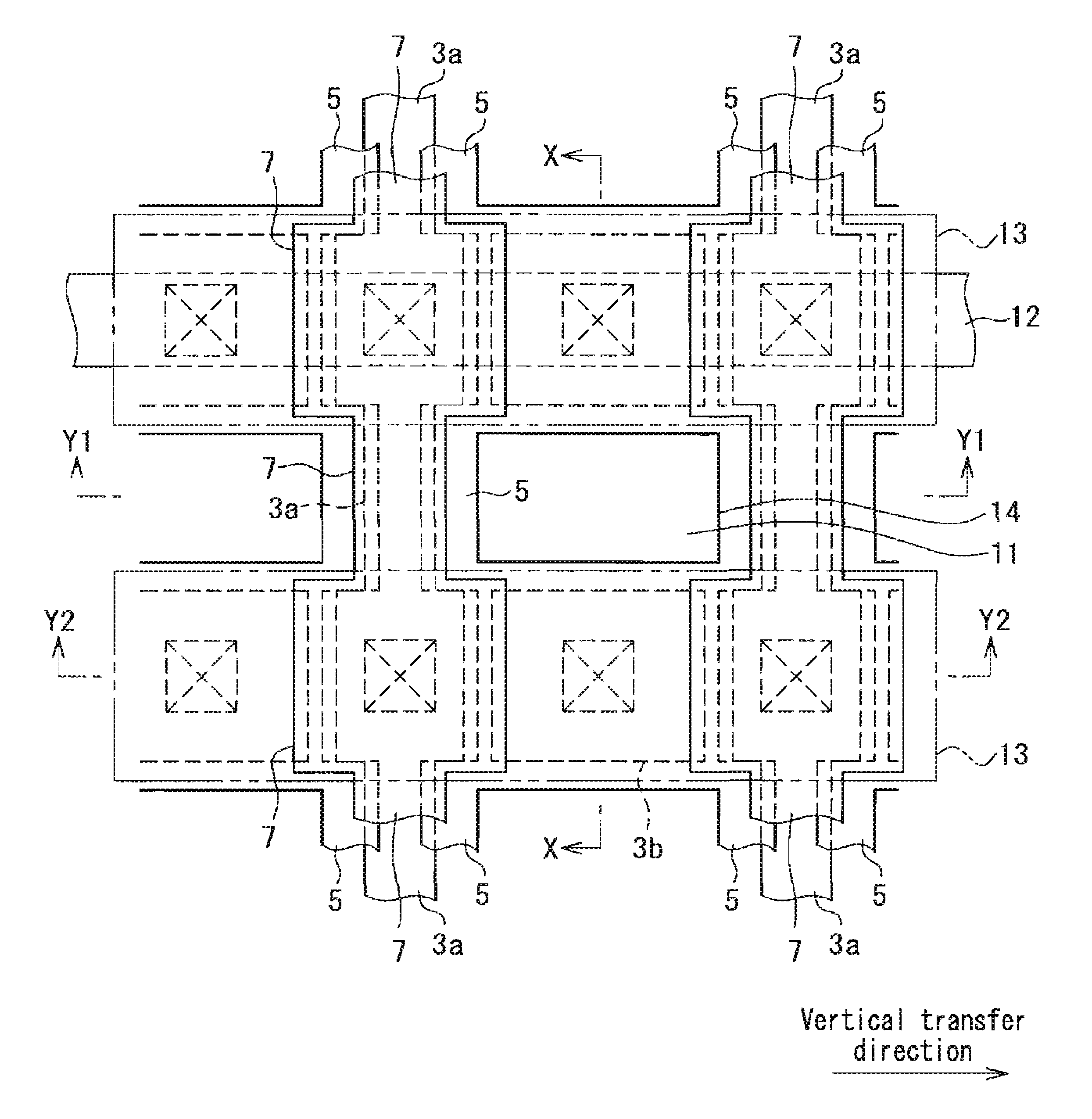
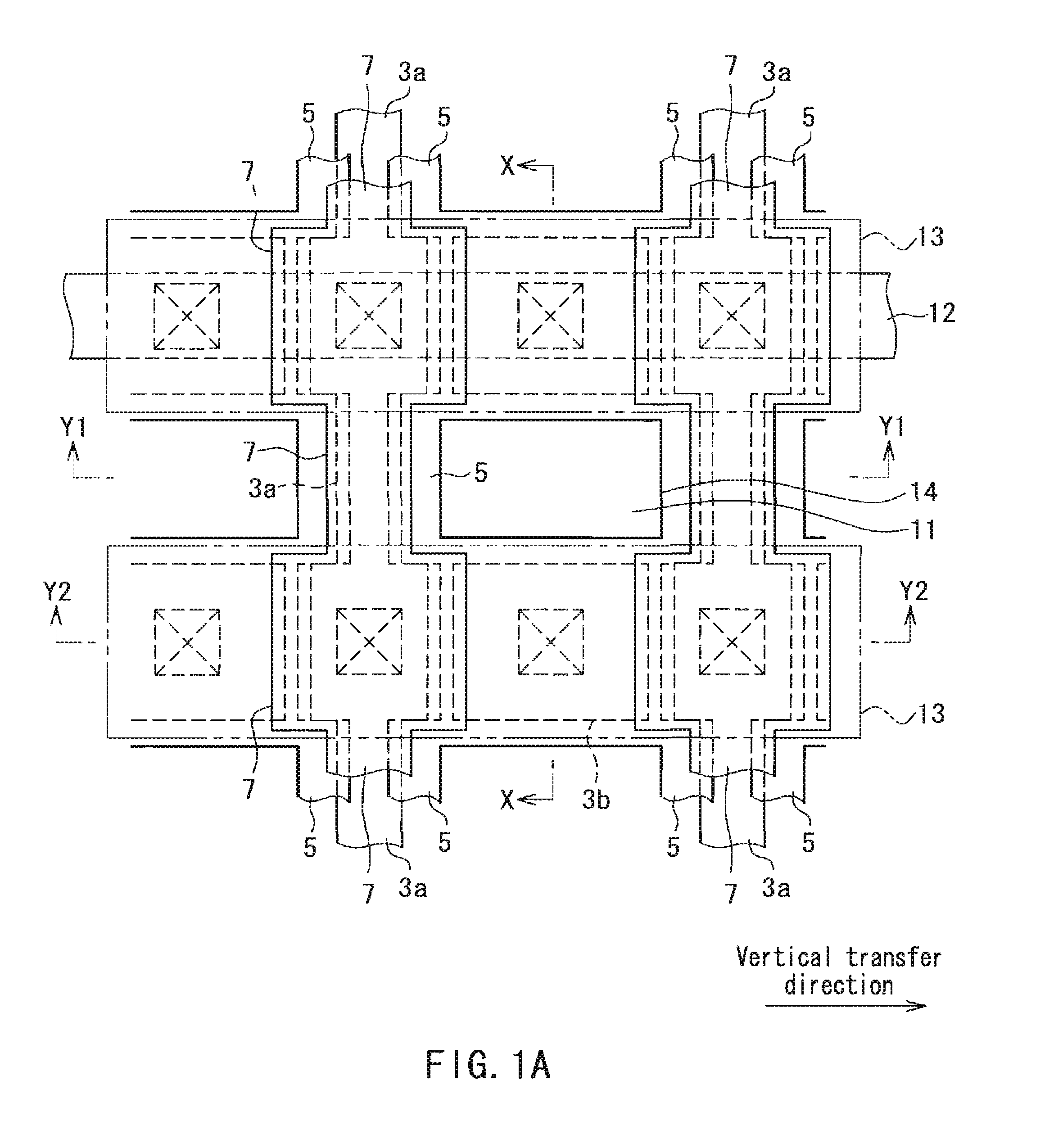
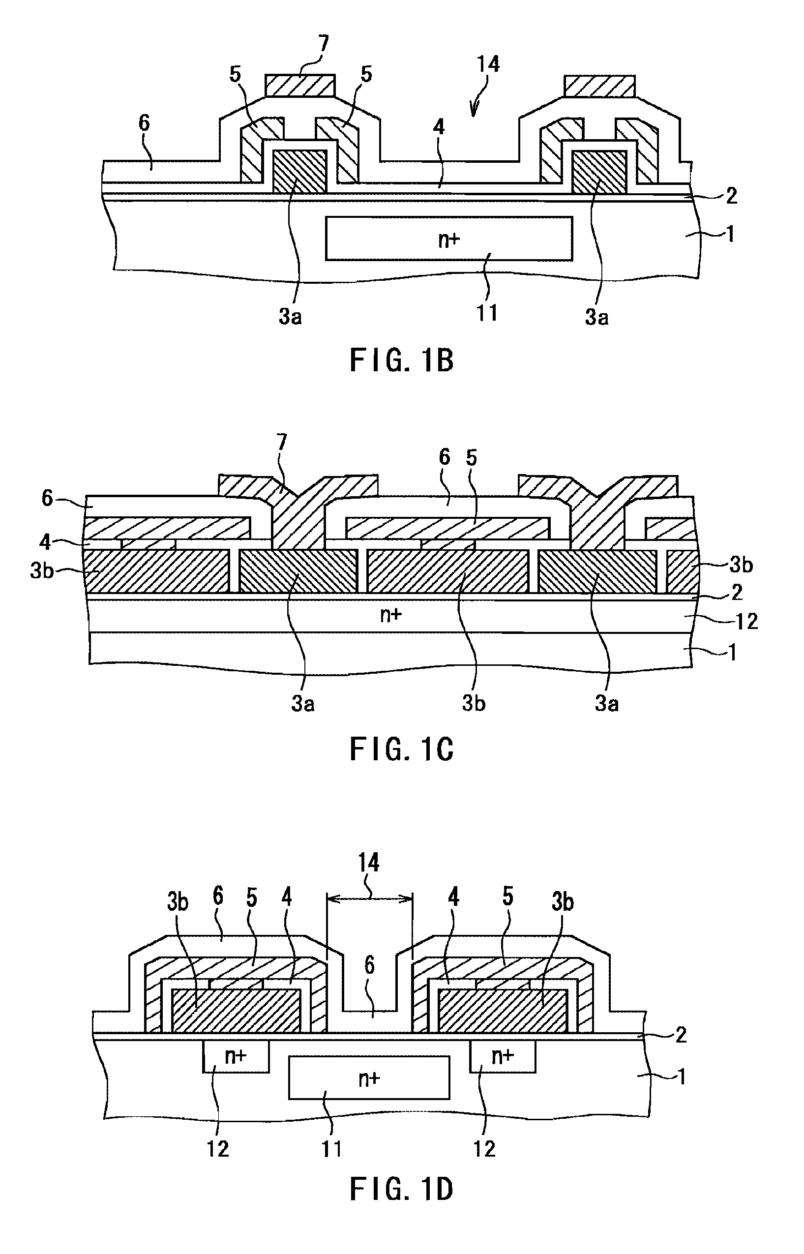
[0045]A solid state imaging device according to Embodiment 1 of the present invention will be described below with reference to FIGS. 1A-3D. The solid state imaging device according to the present embodiment is a CCD type solid state imaging device having a shunt wiring structure. In the present embodiment, a light-shielding film provided on the upper layer of vertical charge transfer parts so as to be isolated in the vertical transfer direction. The light-shielding film shields optically the vertical charge transfer parts and also functions as a shunt wiring for applying a transfer pulse to transfer electrodes.

[0046]FIG. 1A is a magnified plan view showing a portion of a solid state imaging device according to the present embodiment. FIG. 1B is a cross-sectional view taken along a line Y1-Y1, FIG. 1C is a cross-sectional view taken along a line Y2-Y2, and FIG. 1D is a cross-sectional view taken along a line X-X.

[0047]In the solid state imaging device shown in FIGS. 1A-1D, 11 denote...

embodiment 2

[0078]A solid state imaging device and a method of manufacturing the same according to Embodiment 2 of the present invention will be described below with reference to FIGS. 10A-11C. First, the configuration of the solid state imaging device according to Embodiment 2 will be described with reference to FIGS. 10A-10C. FIG. 10A is a magnified plan view showing a portion of the solid state imaging device according to Embodiment 2, FIG. 10B is a cross-sectional view thereof taken along a line Y1-Y1, and FIG. 10C is a cross-sectional view thereof taken along a line Y2-Y2. Components common to those shown in FIGS. 1A-1D are assigned with the identical reference numerals in order to avoid repetition of explanation.

[0079]As shown in FIGS. 10A-10C, the solid state imaging device according to the present embodiment also is a CCD type solid state imaging device having a shunt wiring structure similar to the solid state imaging device according to Embodiment 1. Similarly in the present embodimen...

embodiment 3

[0097]A solid state imaging device and a method of manufacturing the same according to Embodiment 3 of the present invention will be described below with reference to FIGS. 12A-12C. FIG. 12A is a magnified plan view showing a portion of the solid state imaging device in Embodiment 3, FIG. 12B is a cross-sectional view thereof taken along a line Y1-Y1, and FIG. 12C is a cross-sectional view thereof taken along a line Y2-Y2. Components common to those shown in FIGS. 10A-10C are assigned with the identical reference numerals in order to avoid repetition of explanation.

[0098]First, the configuration of the solid state imaging device according to the present embodiment will be described. As shown in FIGS. 12B and 12C, the solid state imaging device according to the present embodiment also is a CCD type solid state imaging device having a shunt wiring structure similar to the solid state imaging devices according to Embodiments 1 and 2. Similarly in the present embodiment, a lattice-like ...


PUM


Abstract

A solid state imaging device has a plurality of photodetector parts 11 arranged in matrix, a plurality of vertical charge transfer electrodes 13 that read out signal charge from the photodetector parts and transfer the signal charge in the vertical direction, and a first light-shielding film 5 that shields the plural vertical charge transfer parts from incident light. Each of the vertical charge transfer electrodes includes: a transfer channel 12 provided along the vertical array of the plural photodetector parts, a plurality of first transfer electrodes 3a that are formed on the transfer channel so as to traverse the transfer channel and that is coupled in the horizontal direction in spacing between the photodetector parts; and second transfer electrodes 3b provided on the transfer channel and arranged between the first transfer electrodes. The first light-shielding film is formed continuously in the horizontal direction and has openings formed on the photodetector parts. Isolation regions having electroconductivity are formed between the photodetector parts and connected electrically to the second transfer electrode. Thereby, a shunt wiring structure capable of a high-speed transfer at a high sensitivity and with reduced smearing is obtained.

Description

BACKGROUND OF THE INVENTION[0001]1. Field of the Invention[0002]The present invention relates to a solid state imaging device having a configuration for transferring a signal charge read out from photodetector parts arranged in matrix, through vertical charge transfer parts. The present invention relates also to a method of manufacturing the solid state imaging device.[0003]2. Description of Related Art[0004]Solid state imaging devices represented by a CCD (charge coupled device) type solid state imaging device have been used widely as imaging elements for imaging apparatuses such as digital still cameras and digital video cameras, and the demands have been increased even more. In addition, due to the demands for coping with moving video pictures of high-definition TV in an imaging device accompanying a trend for the high-definition TV, enhancement in the speed of the transfer frequency has been required for such a solid state imaging device.[0005]As a technique for enhancing the sp...

Claims


Application Information

Patent Timeline
Patent Type & Authority Patents(United States)
IPC IPC(8): H01L27/14
CPCH01L27/14818
Inventor MIZUNO, IKUOYAMADA, TOHRU
Owner PANASONIC SEMICON SOLUTIONS CO LTD
Why Eureka
Try Eureka